Introduction
In Part 2, we finished picking out all of the major components for our outdoor, PoE-powered microphone project. In this part, I’m going to walk through the next steps that I like to take to break down the scope and ambiguity into smaller chunks.
My goal here will be to make 2 or 3 test boards in order to familiarize myself with the components, and minimize component waste. Mistakes will be made - and I don’t want a mistake in my MCU design to mean that I have now stranded a bunch of other components on the same board that, without a working MCU, I can’t even test to see if I’ve laid them out right or not.
There’s also a pipelining advantage. PCB fabrication takes at best a few days, sometimes a couple of weeks. I’d like to get one of those fired off ASAP, then work on other unrelated designs as I’m waiting for the PCB, and components, to arrive. Small boards are also cheaper to iterate on - so cheap that I generally don’t hesitate to order expedited service.
All that said - let’s pick a component to start with. I’m going to go with our MEMS microphone part, the SPH0645LM4H-B, for a couple of reasons:
- It’s standalone, presenting an I2S interface on two of its pins. I happen to have a Sparkfun ESP32 Thing lying around, which being an ESP32 part has I2S support. So this gives me something I can test the breakout board with.
- It’s really simple, just a few components, so that’ll be just an evening’s work to design and order, which will give me some momentum.
The PoE controller I’ll be able to make its own breakout board for - after all, it’s just a power source, and that’s something easy to see if it’s working or not - but the Ethernet PHY and MCU might have to be on a test board together, as I have nothing else lying around that knows how to speak RMII to it.
Now - let’s move on to actually designing the first breakout board.
Design Toolchain
My goal with this writing isn’t to be a comprehensive tutotial on how to use these tools - there are way better tutorials and learning resources out there.
When I started out, I followed the Sparkfun EAGLE tutorial. If I’m being honest, probably the right thing for someone trying this out new would be to use the open-source KiCad, but I’m just a little too used to the EAGLE workflow and where all the buttons are, so I haven’t migrated myself (EAGLE has actually been folded into Autodesk Fusion 360, so that’s what you’ll see here). Broadly, all of these tools work the same way, being made out of 3 things:
- A logical PCB design schematic of how your components are connected outside of their physical relationship - e.g. “the 3.3V-input pin of this MCU is connected to logical GND via a 0.1uF capacitor”.
- A component library that maps logical pin descriptions (e.g. “the 3.3V-input pin”) to the specific solder pad or pads in a physical diagram of the exact dimensions of the component’s footprint on the board.
- A physical PCB layout of these components that you have physically placed in relation to one another, and drawn wires between to match the logical relationship in the schematic.
EDA programs such as EAGLE or KiCad tend to come with their own component libraries, but the space of available components out there is so vast that outside of standard passives - every 0603-sized resistor is completely identical from a schematic and dimensions perspective - I tend to reach first for third-party resources. As it turns out, our MEMS microphone part has an available library on SnapEDA. This will give us the schematic diagram of the microphone, the physical footprint, and even a 3d model (which isn’t just for fun - particularly in a tool like Fusion 360 which makes this integration relatively seamless, having a full 3d model of your PCB is invaluable for designing surrounding parts like enclosures).
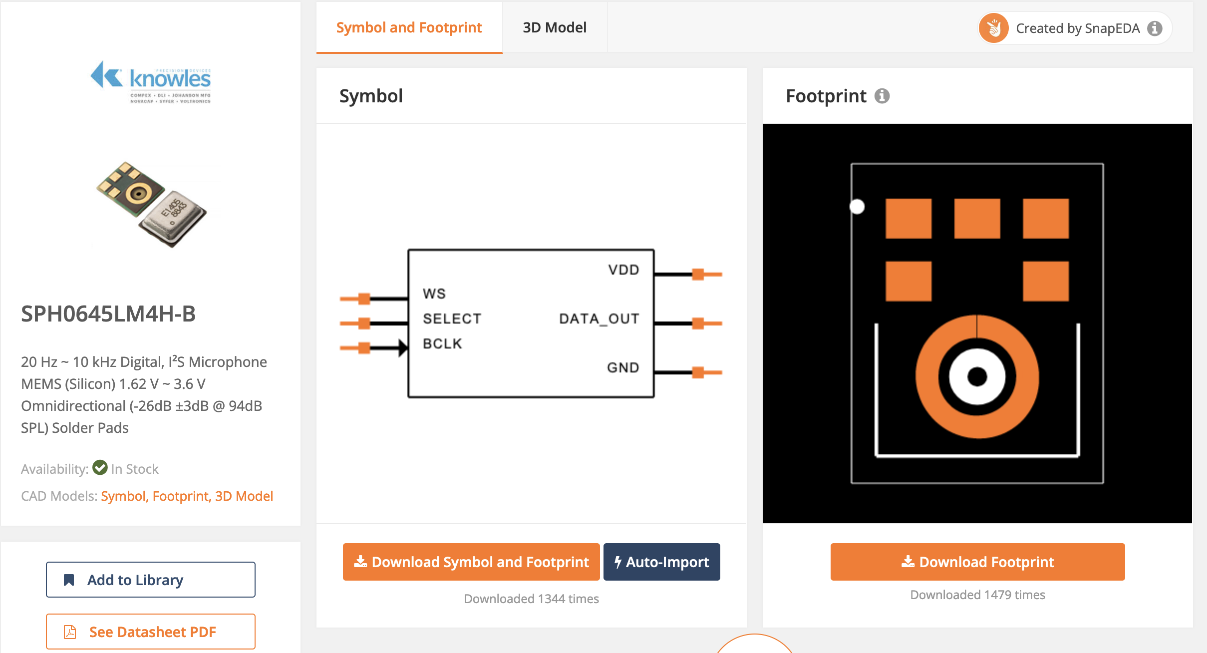
This gives us a starting point. The next thing we need is an idea of the basic connections that this part requires - for that we go to the datasheet.
Datasheet Walkthrough
Every component you put onto a PCB has a datasheet. I think of a component (like this microphone) as analogous to a software library - it’s a thing that was built by someone with deeper domain expertise than you, who put an accessible interface in front of it so you can write glue that composes it together with other things. The datasheet is the documentation - setup instructions, any necessary dependencies, thresholds and limits, expected performance, and the interface itself. Many also come with examples - and this one does, a really nice one:
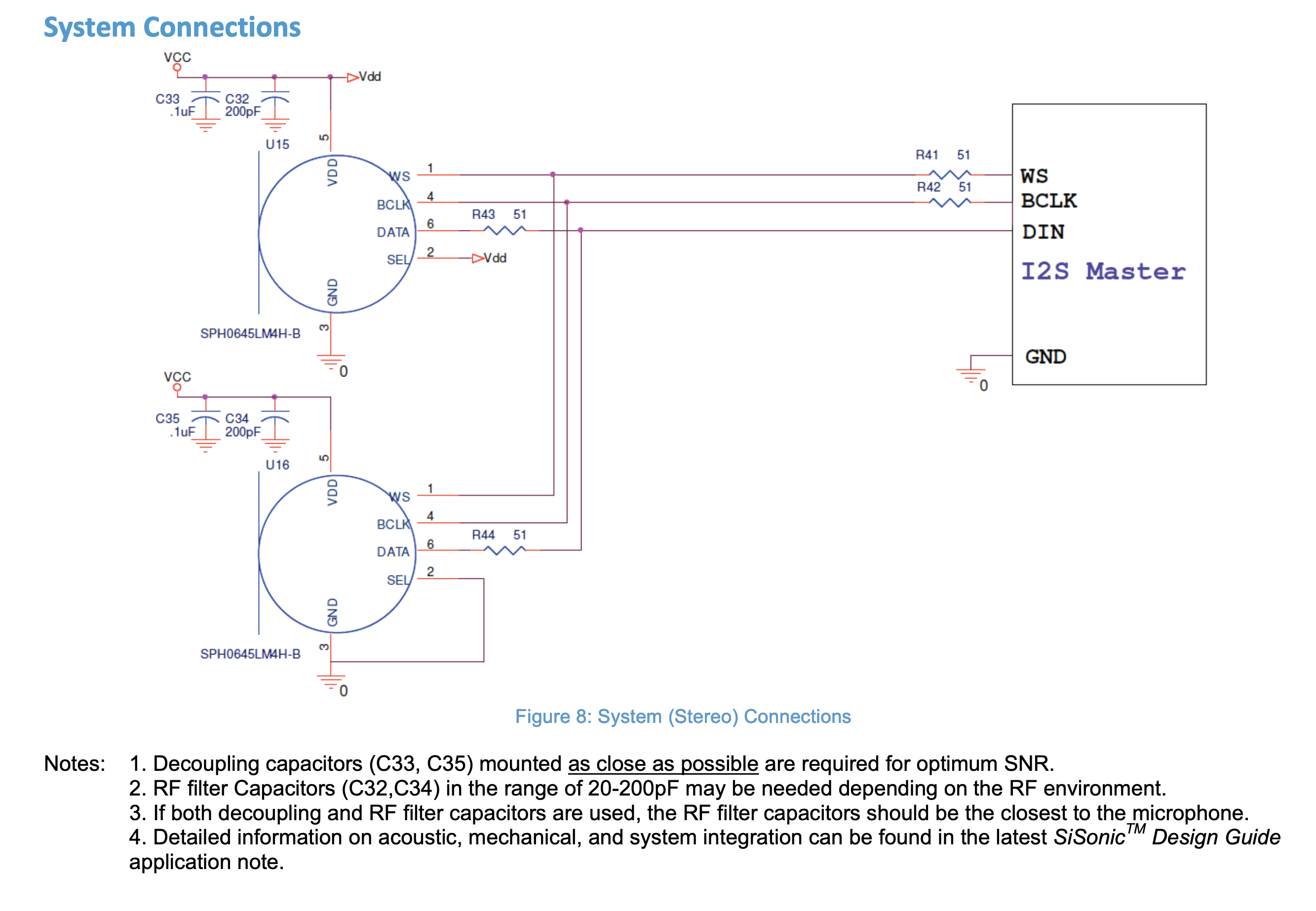
This basically tells us everything we need to do. It’s in a stereo configuration here - the WS signal in I2S is essentially an ‘enable’ signal that the MCU controls flipping back and forth. We’re just doing mono here, so we’ll just run WS right to the MCU (or in the case of this breakout board - just a pin header we’ll wire to the ESP32 Thing).
If I were looking at one of these for the first time, I’d have a few questions that these days I can answer:
What are VCC and VDD?
There’s a long story here, but broadly, VCC and VDD are shorthands for “supply voltage”. You might see VSS in some datasheets - this is similarly shorthand for the ground reference.
What are those capacitors by VCC (C33 and C32)?
These are decoupling capacitors. It’s worth googling this and reading more. Basically - every IC that’s going to have irregular needs for current (and if you think - that will be at least everything that has a clock signal, which this part certainly does) needs capacitors to store some local electrons to keep spikes in current demand from dropping the voltage on the power rail. Basically - it’s like a little cache so the IC doesn’t have to go all the way to the database (in this analogy, that’s the actual power supply, and to be more specific, that’s really just the next closest capacitor).
These are also often called ‘bypass capacitors’. Usually datasheets will offer recommendations for values and which pins need them (generally this is all power supply pins). I usually CTL-F for “decoupling” and “bypass” in the datasheet as one of my first steps in adding support components to a schematic. As you can see - this schematic diagram in the datasheet calls out these capacitors explicitly, pointing out that they should be laid out as close to the VDD pin as possible, which makes sense - you want a close cache!
Notably the capacitors are of two different values - this isn’t all that uncommon. I don’t claim to have a super deep understanding of why - this Sparkfun tutorial goes into more detail and is worth a read. But - the good news is that this kind of stuff has been figured out by the engineers who designed this IC and helped write the datasheet, and we can just do what they suggest.
What are those resistors on the data lines? Don’t resistors ‘slow things down’?
Good question! Series (i.e. inline) resistors are pretty common on high-speed data lines. USB lines, for example, all have 22Ω resistors. Similar to the above - there’s a lot of theory behind it (here’s a good starting point). In a high-level, handwave handwave sense, while there are many textbooks written on high-speed signals and impedance (i.e. handwave handwave ‘resistance’), the end result is you add a generally very low-resistance series resistor to make the overall signal path all ‘the same’. Again - at a super high level, I get it, and the nice thing is the datasheet doesn’t just assume I already know about it.
Schematic Design
The first thing we’ll do in our “New Electronics Design” (in Fusion 360 language) is pop our new component into the schematic pane:
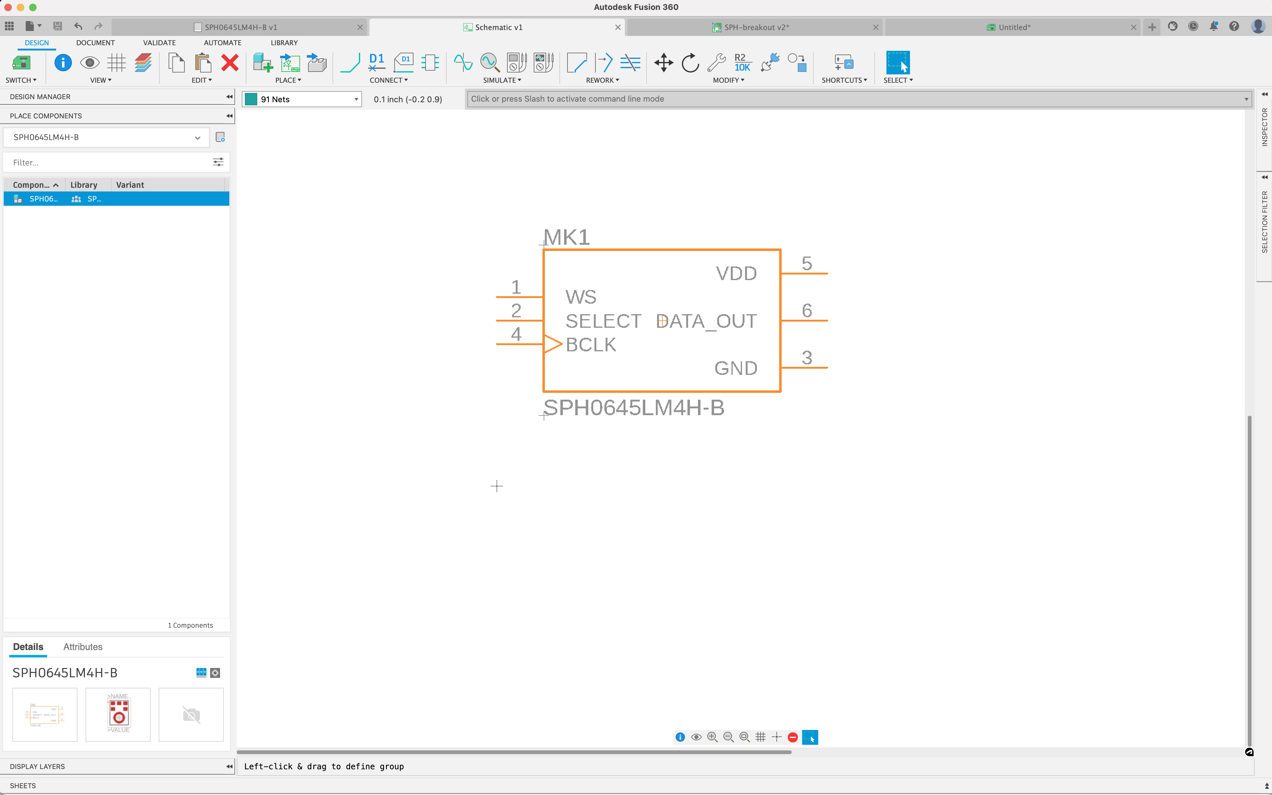
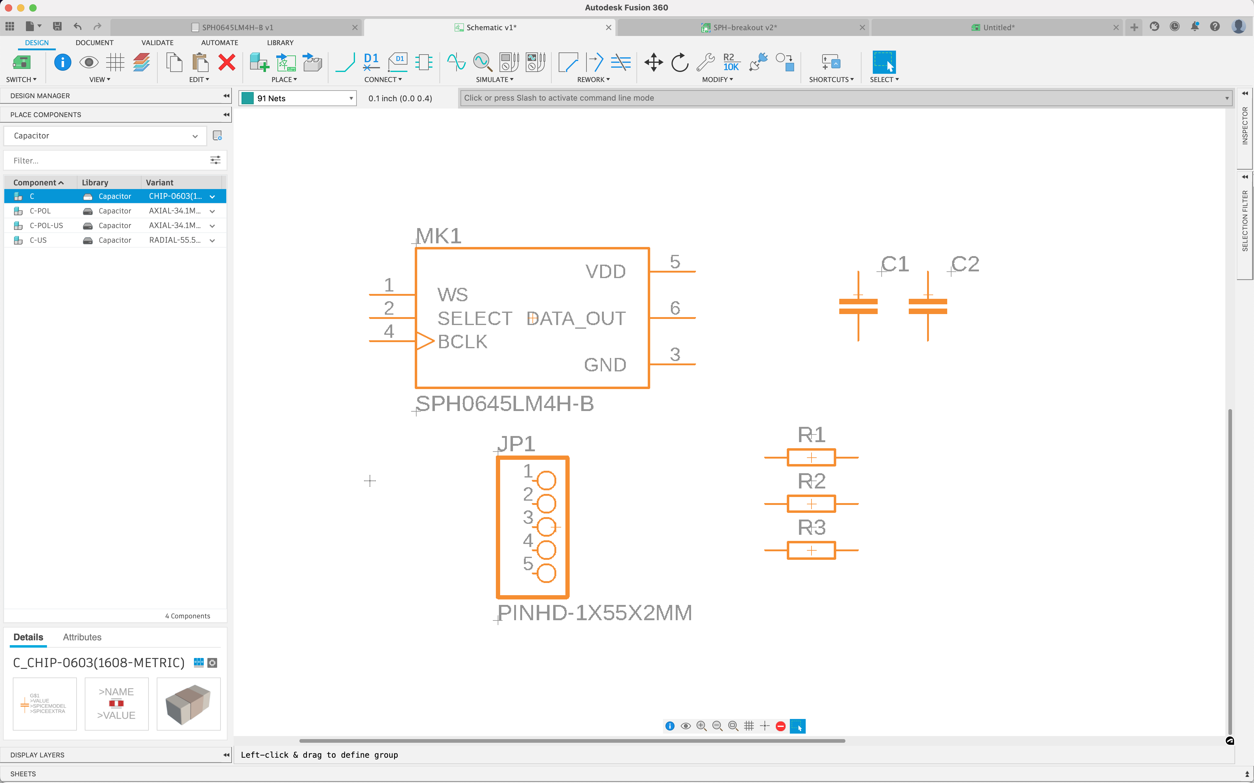
Then we need just a few things:
- 51Ω resistors on the WS, BCLK, and DATA lines.
- 200pF and 0.1uF capacitors for the power input.
- A 5-pin standard 0.1” pin header for the WS, BCLK, DATA, VCC and GND connections.
For the resistors and capacitors, I’m using the “Resistor” and “Capacitor” component libraries built in to Fusion 360. Fusion also has a ‘Connector’ library that has the pin header.
I’ll then go through, clean things up, make wire connections between the components, and add +3.3V and GND signals:
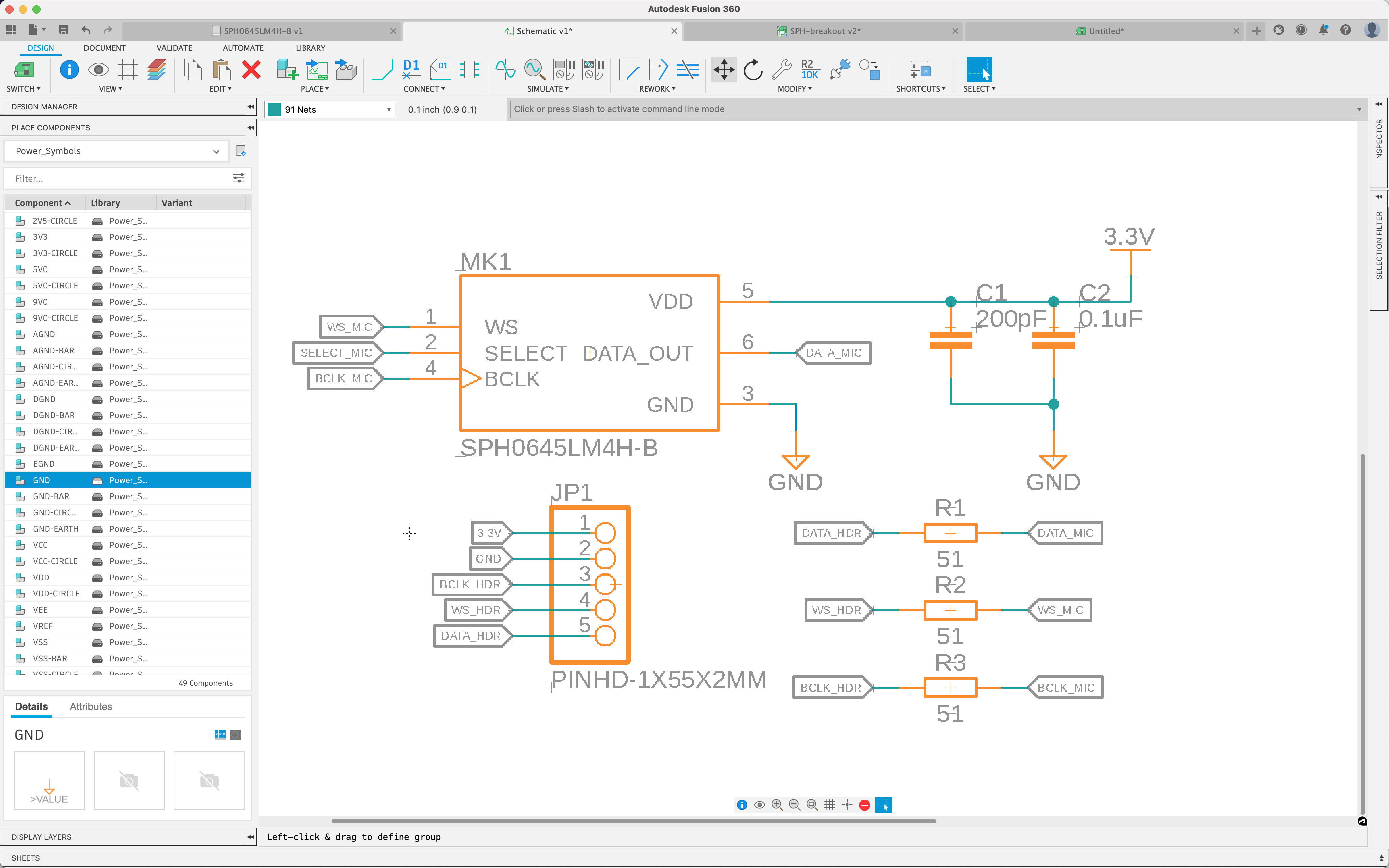
Remember that none of this has any bearing on the physical layout of the board. Schematics should be optimized for readability. Many people do a way better job than me at this - I’m letting myself be a little bit sloppy here since this is just the breakout board.
Passive Component Selection
One thing that you have to decide on when laying down passive components is their size. I want to take more time to write about component selection in another post, but I generally follow these rules of thumb:
- All resistors 0603.
- Capacitors 0.1uF and under size 0603.
- Larger capacitors (1.0uF or 4.7uF) might be 0805 or 1210.
Generally - at low voltages I don’t see resistor size as something that really matters, and 0603s are pretty easy to work with. Too-small capacitors tend to not operate at their rated capacitance at high enough voltages, but too-large capacitors respond more slowly. Unless the datasheet recommends otherwise - or space requirements force me - I tend to stick with these rules of thumb. As a result, all of these passive components are 0603.
PCB design and layout
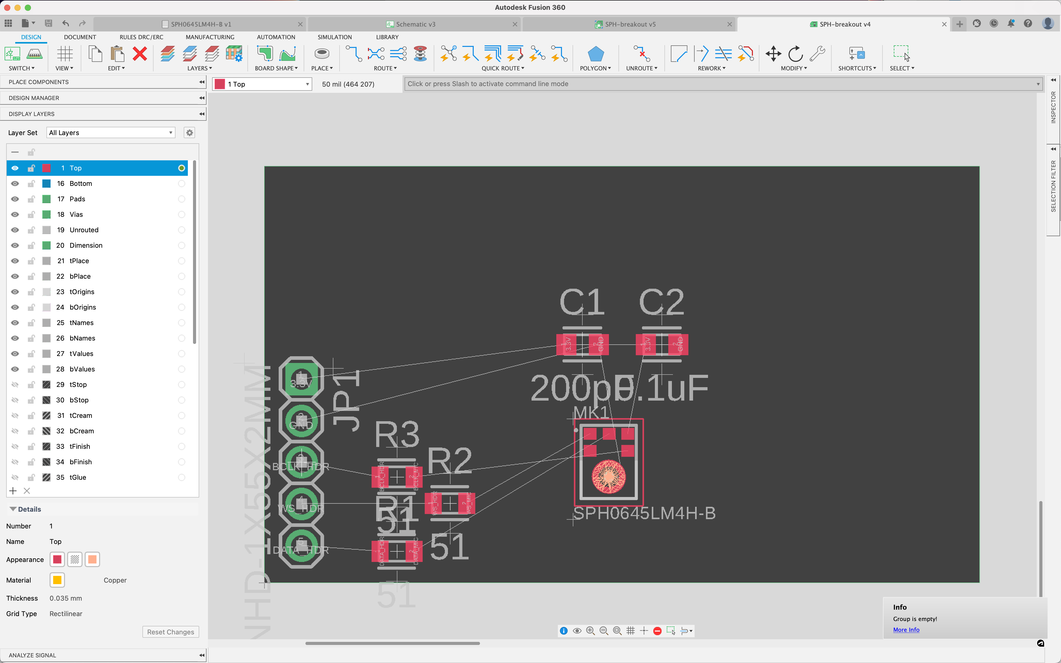
Let’s move over to the PCB layout. The first thing that we see when we switch to the board layout pane is a bunch of components with “airwires” (logical connections) between them:
Then I typically do a quick and dirty shrink of the board footprint to about the right size, and rough placement of components:
Note that there are thin ‘airwires’ representing the schematic lines. One measure of whether a board is ‘done’ is when all of those airwires are gone - replaced by wires drawn in explicitly. After laying those out and another round of cleanup:
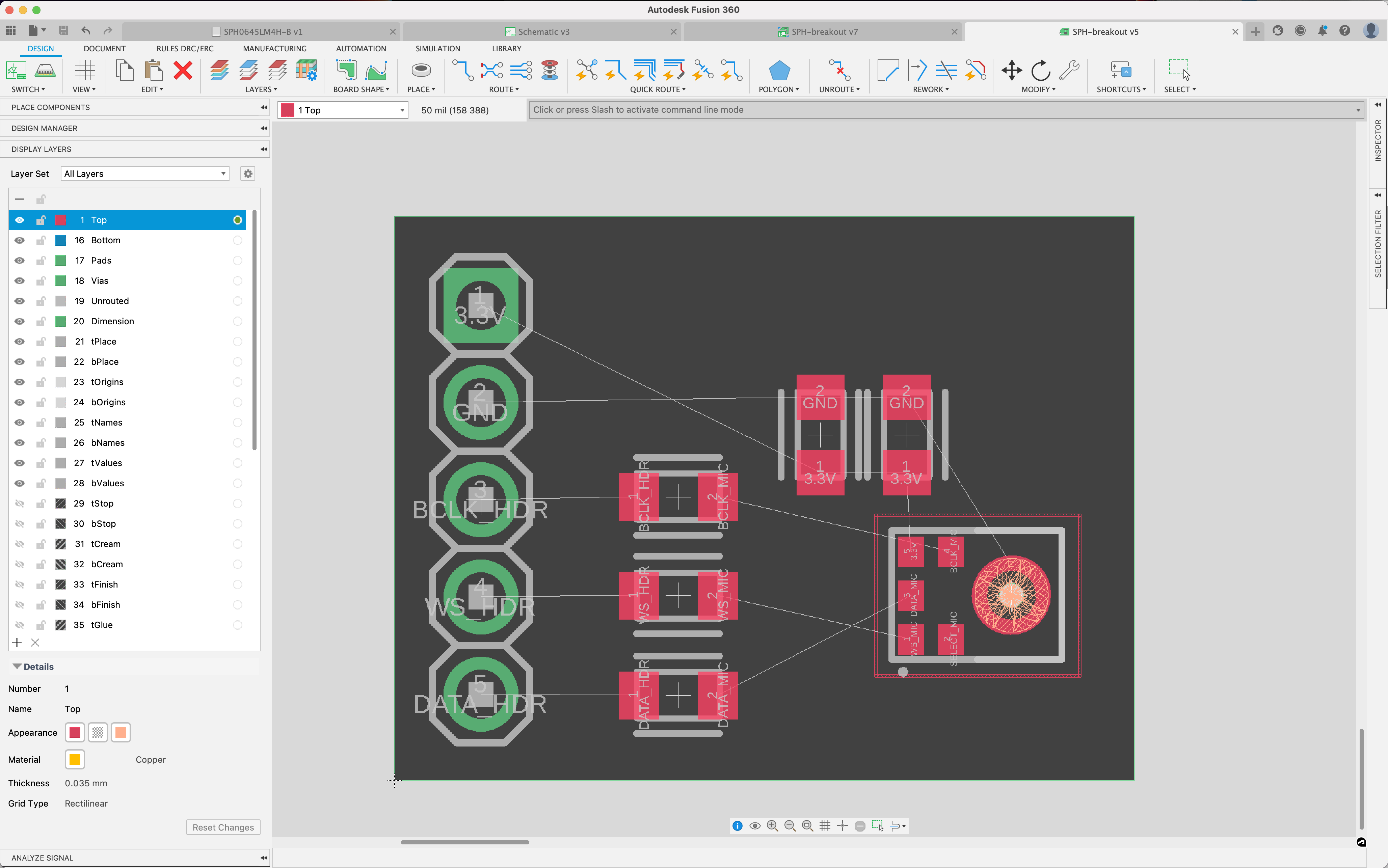
Here’s something that happens all the time - I was completely winging it when I picked which signal was going to run to which header pin, but now it looks like that’s going to be pretty inconvenient since the WS and DATA lines are crossed. So - we’ll need to switch back to the schematic and change the order of those pins on the header, then after rearranging the components, we can start making some wires.
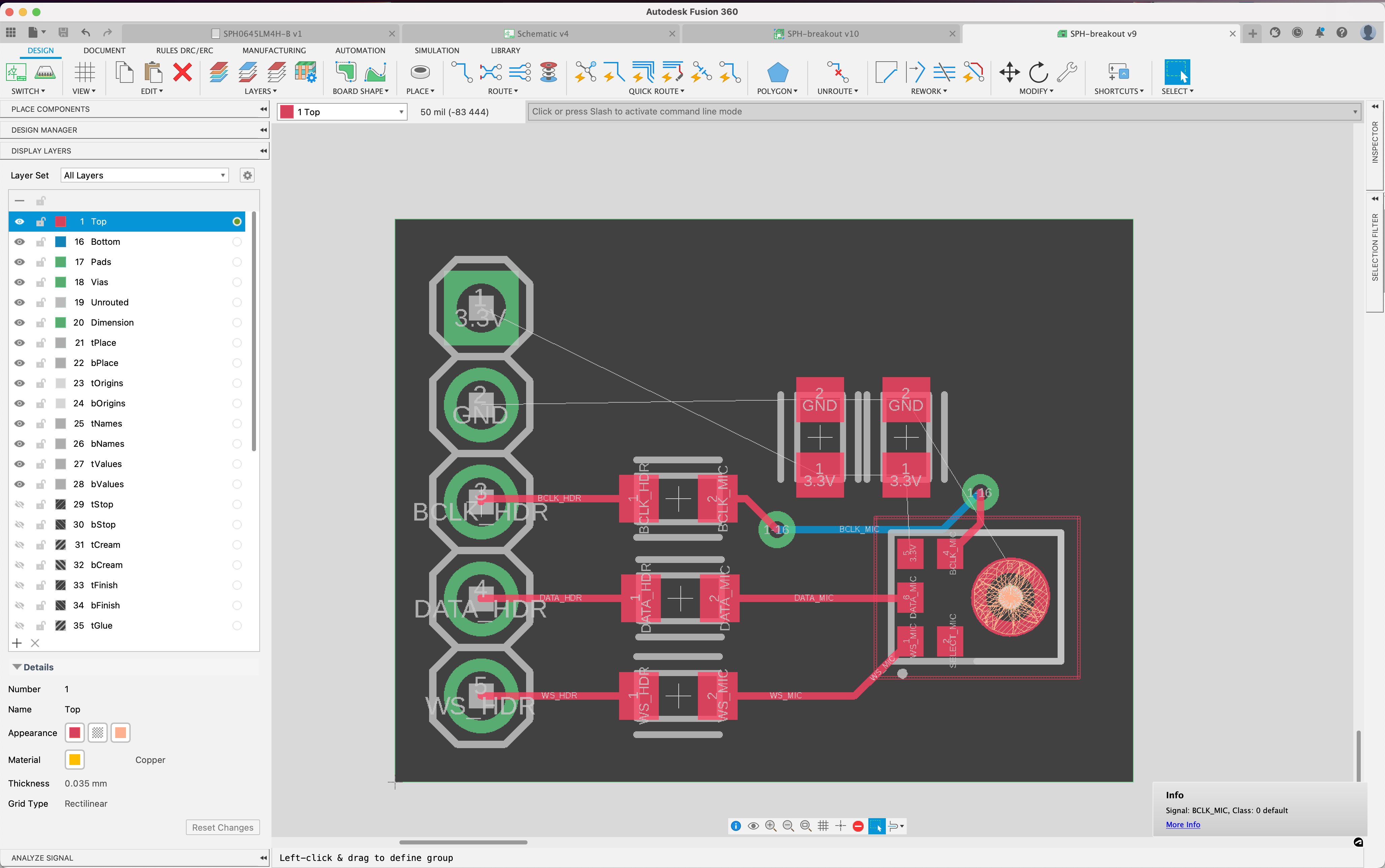
Note - we had to pass one of the traces to the other side of the board so that we can reach those capacitors from the power pin. After doing some polygon pours - the whole top layer being GND and the whole bottom layer being 3.3V - we are faced with a new problem:
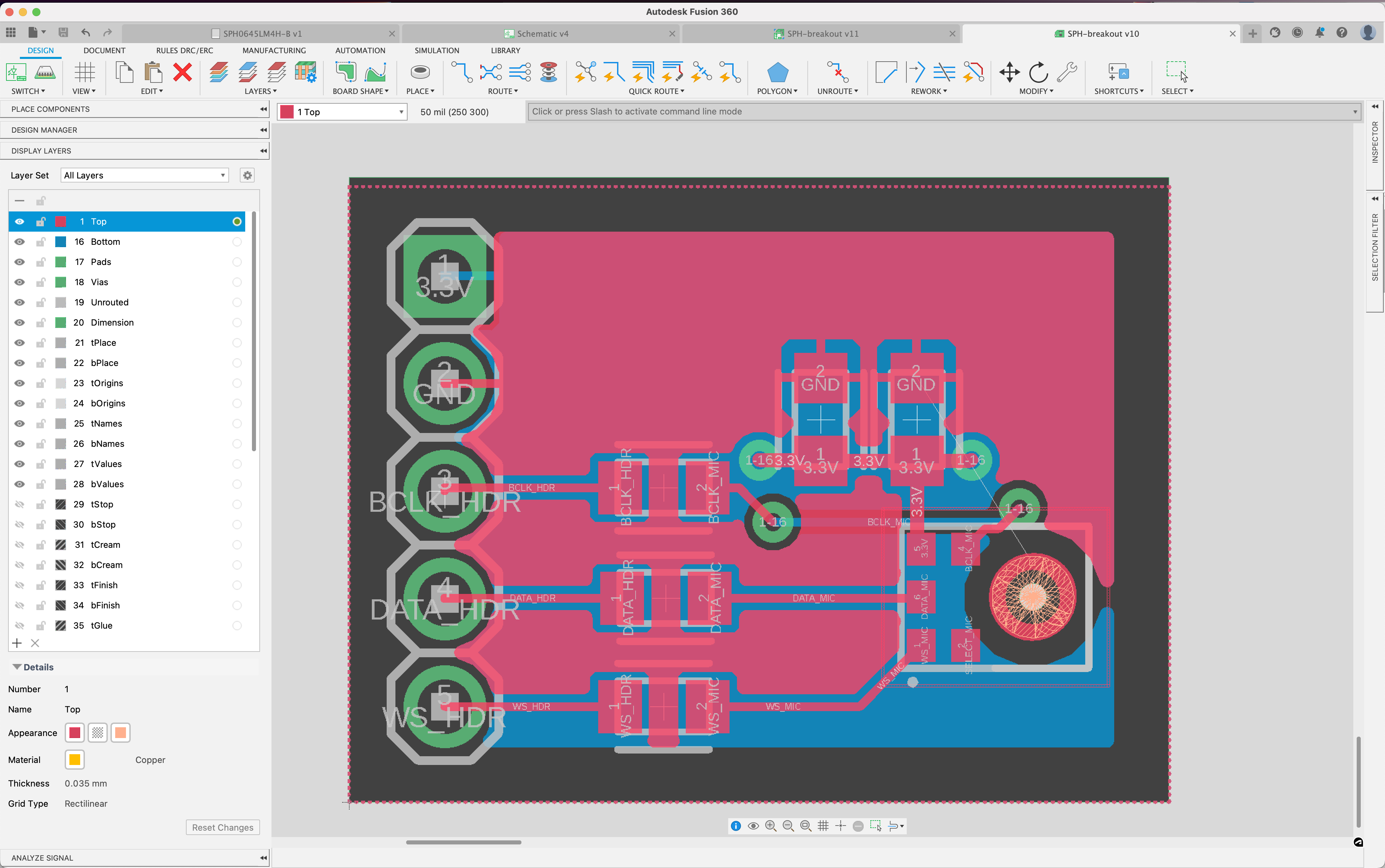
The footprint for the mic has a board edge cutout for the center hole, and our board settings prohibit any copper pours or traces close to board edges. We can fix this - since this is something that is up to the tolerances of the fabricator, though, we want to use the file OSHPark provides here. We can load this into Fusion 360 and run a full DRC (Design Rules Check) to get Fusion to re-check. We can also add some silkscreen documentation annotations, like the board version and the labels for the header pins:
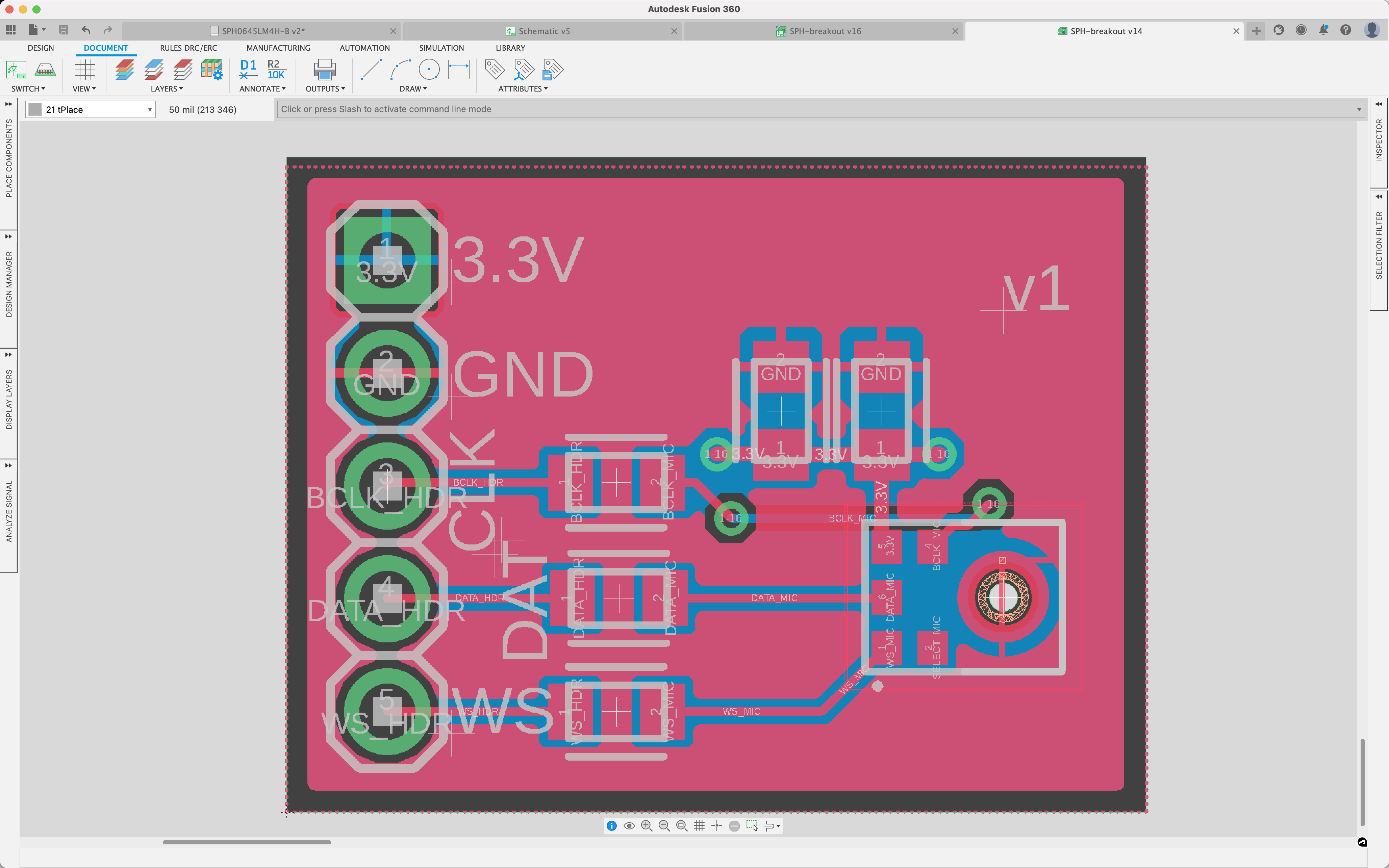
I think we’re now ready to order the board!
Fabrication Toolchain
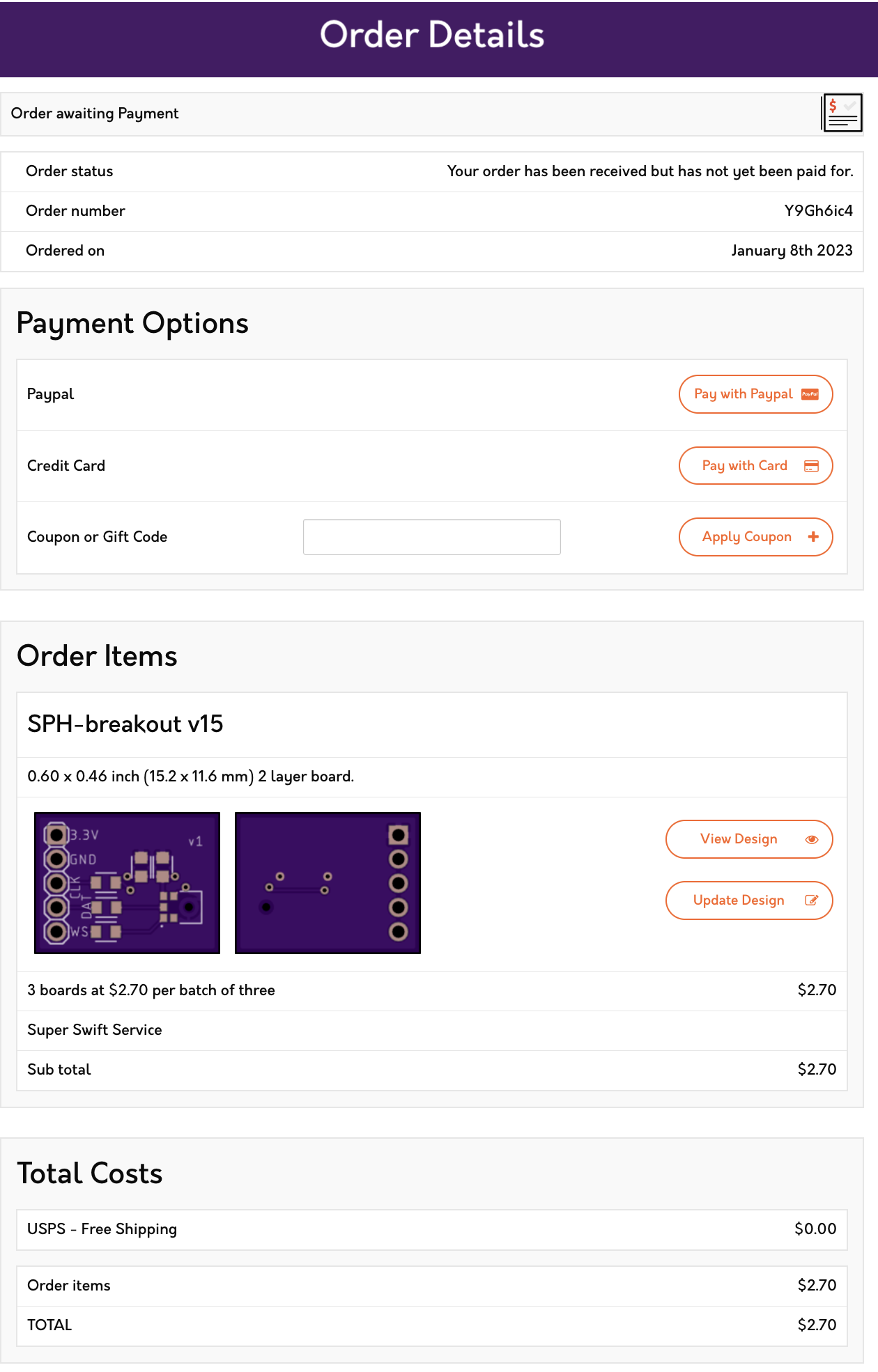
I like to use OSH Park for PCB fabrication. They integrate directly with .brd files that EAGLE (and now Fusion 360) can export. It’s a pretty easy process that gives you preview images - and has free shipping!
$2.70 all told for the ‘super swift’ service of this tiny, 15x12mm board:
That can wrap it up for this part - in Part 4, I’ll go into ordering and organizing the components and solder stencil for this board so that it will be ready for assembly.