Introduction
The PCBs, stencils, and components for the microphone breakout that I ordered in Part 4 have all arrived, which is exciting, but I don’t have time at the moment for doing assembly, so instead I’m going to spend some time digging into the datasheet for our MCU of choice and beginning to work on the schematic for the next test board - one that will bring together the MCU, the PHY, an ethernet port, and some breakout headers for I2S so that if it all works, we can test it against our microphone breakout board without making a new revision. It will also take power through just a couple of header pins (rather than something easier than USB) - so that if we’re successful with our PoE breakout that’ll come later, we might be able to frankenstein the whole setup together!
Generally none of my boards work on the very first try, but it’s never a bad idea to plan for success.
As before, the first thing I’ll do is find CAD files for the part online if they’re available - and it turns out that if you create an account, Microchip will happily give you a .zip with a schematic, footprint, and 3D model. So - loading up all those into a fresh PCB schematic in Fusion 360, I immediately see that this part is a relative doozy:
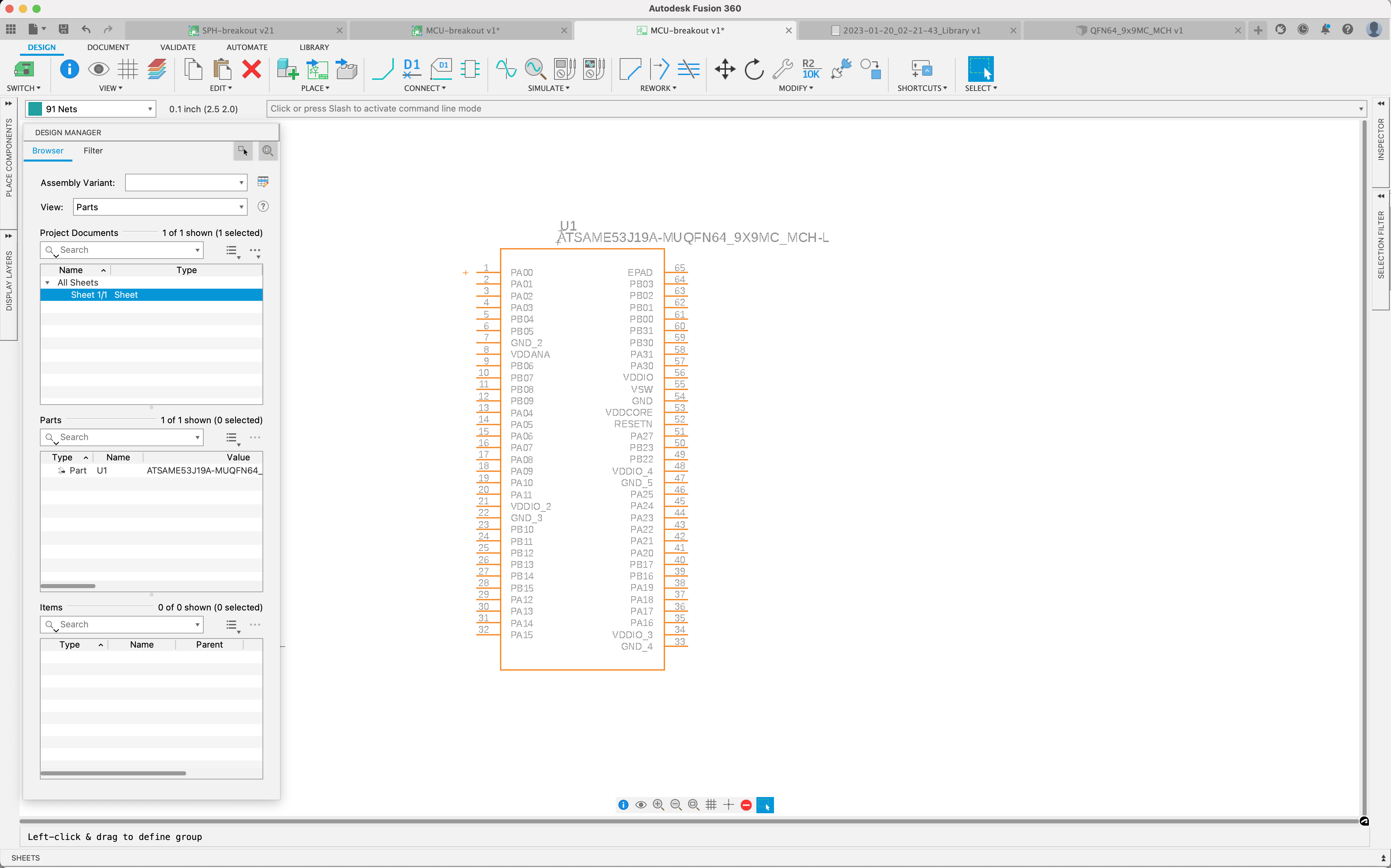
I’ll want to break out 3 signals: the RMII interface to the ethernet PHY, the I2S interface to some pin headers, a serial port for debug operation, and whatever pins I need to use my ATMEL-ICE programmer to actually program this thing.
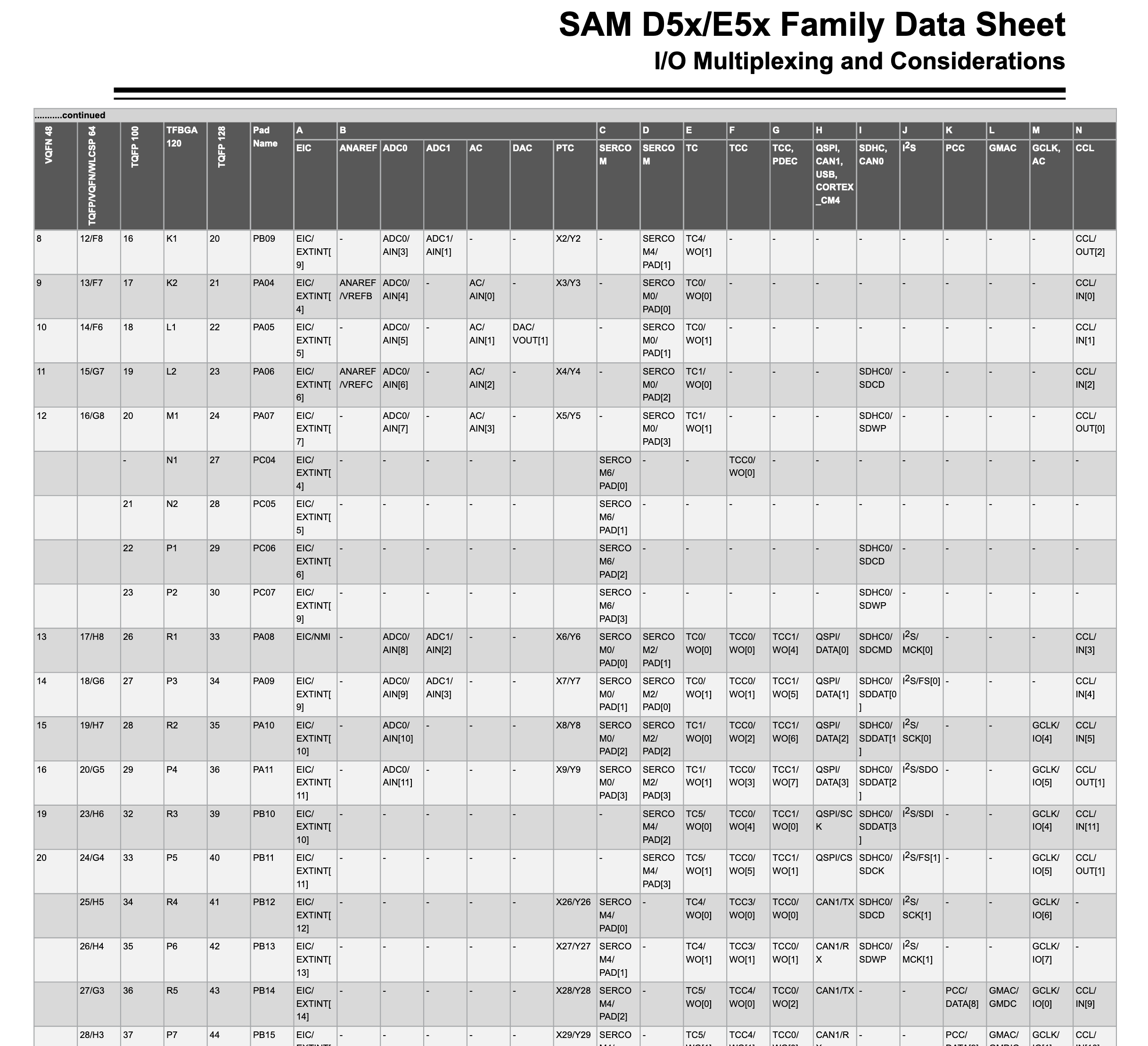
I started by walking through Table 6-1 in the datasheet, which is a pin-by-pin description of what functions that pin supports. Notably - most (maybe all) of the peripherals on this MCU have two different options for the sets of pins they can use (I found this described in 6.2.8 - IOSET Configurations).
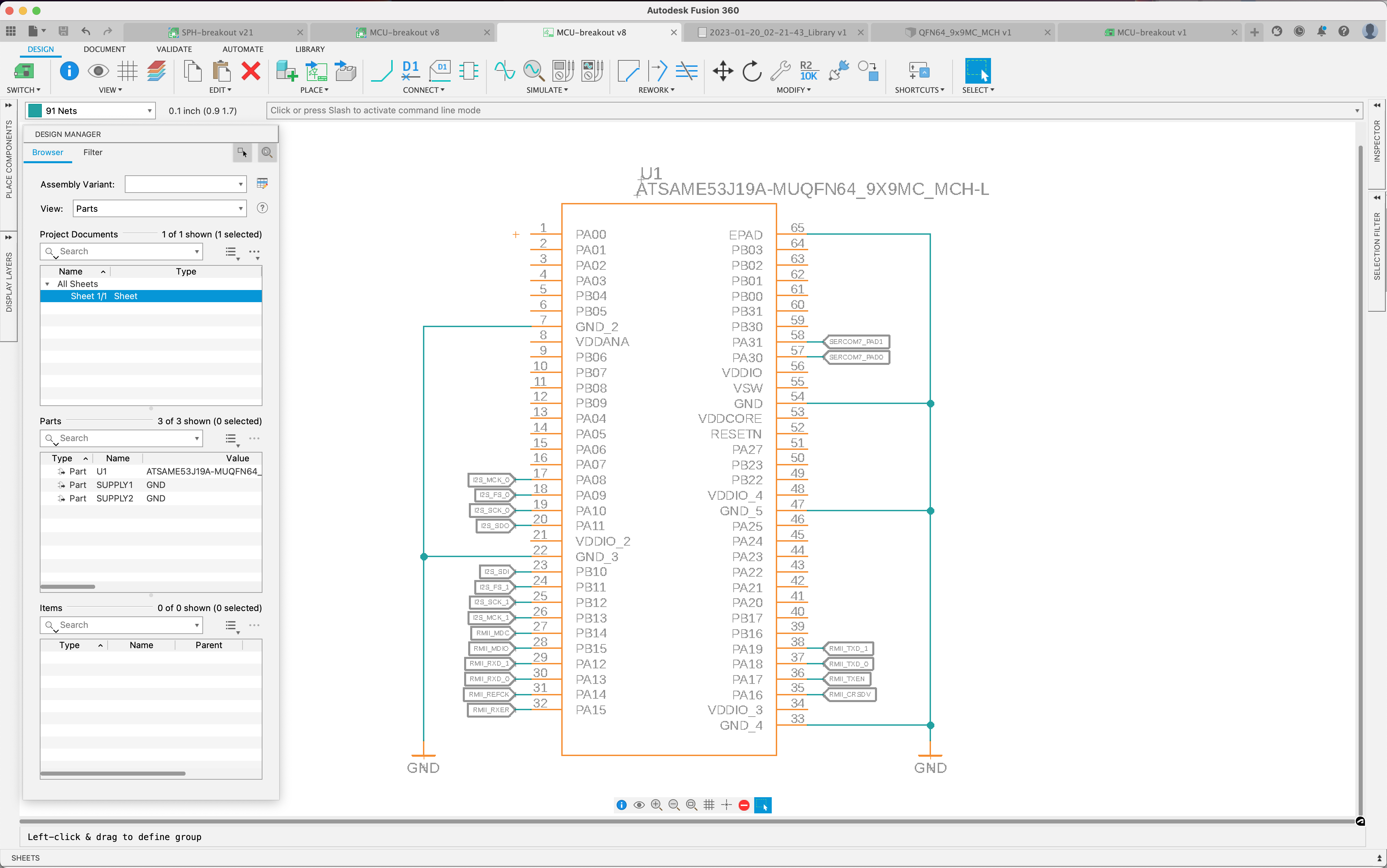
I don’t have a very crowded board, so I think what I’ll do is just pick IOSET 1 for both the MAC and I2S interfaces - these are non-overlapping. I’ll then relatively arbitrarily use IOSET 1 of SERCOM 7 for serial TX/RX (this MCU has 8 distinct serial interfaces) whose pads 0 and 1 are relatively far from the other pins I’m using, in hopes that’ll simplify layout later.
After using the table in Section 24.4 to clean up the GMAC signal names into RMII-specific ones, we have our basic peripherals broken out - plus the GND connections for good measure. This part has an exposed pad on the bottom, described in the schematic as EPAD, and which the datasheet recommends be connected to the PCB GND signal even though it’s not electrically connected inside the device.
The next thing I’ll do is walk through the handy Schematic Checklist in the datasheet, which is going to walk me through any external passive components needed, power supply requirements, any external clock crystals, and the programming pins. Datasheets for simpler ICs typically don’t have these, so thank goodness that this one does.
Power Supply
I’m given a handy-dandy full diagram of the passives and expected voltages of the power supply pins:
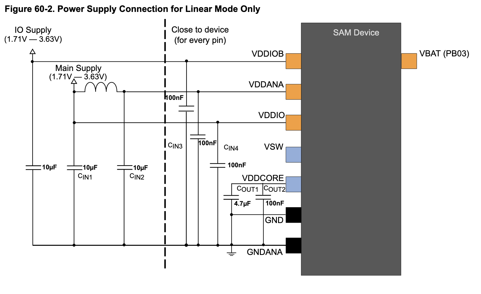
I’ll make a 3.3V net in Fusion, then connect it directly to VDDIO and VDDIOB (on my schematic - I had to double-check - that’s pin 21, labed VDDIO_2). VDDCORE is the output of an internal regulator, and needs bypass capacitors to GND, but not its own supply. VSW and VBAT I get to leave empty, and VDDANA would like a ferrite bead between the supply and the pin, per this app note:
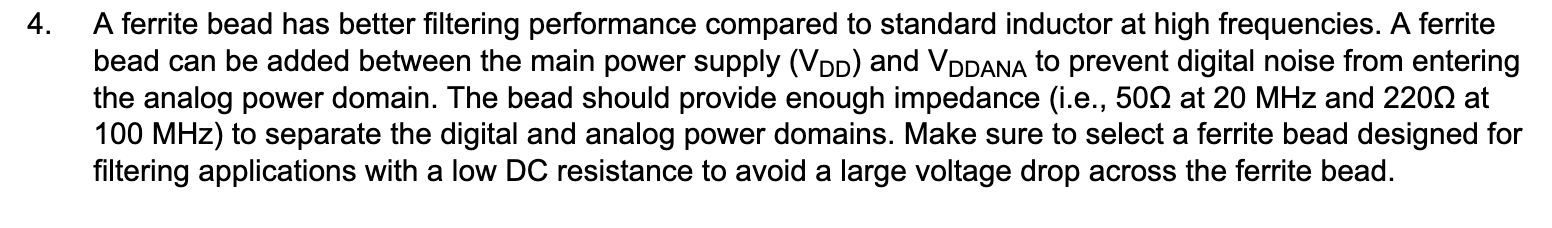
That’ll be important to come back to when selecting passive components. So - with the signals ran, and the pictured capacitors and ferrite bead in place, we’re seeing a much more filled-out schematic:
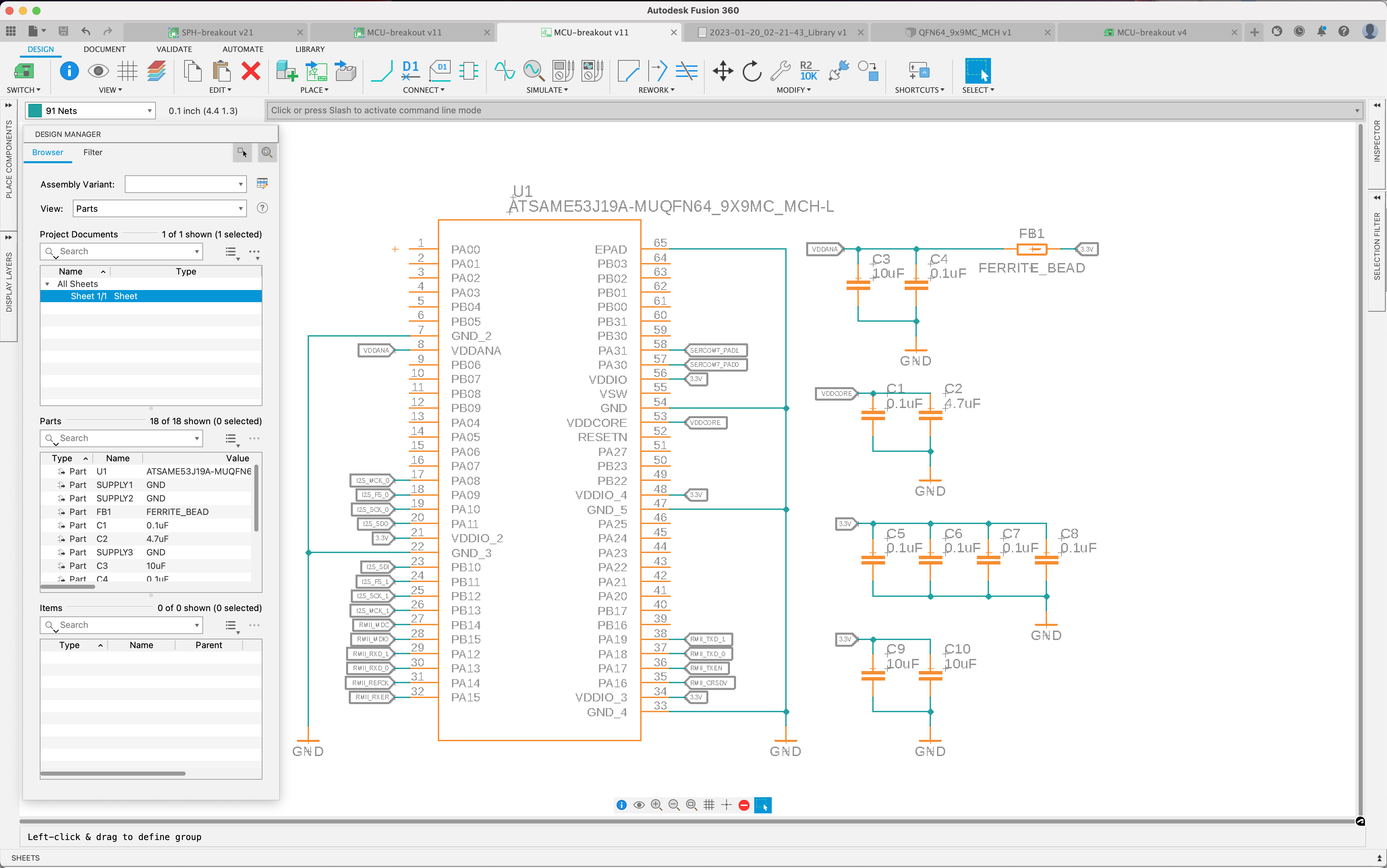
I’ve noticed that the datasheet is a bit ambiguous about where the 10uF capacitors should be - the 0.1uF ones are bypass ones for the VDD pins, and the 10uF ones are for the internal regulator that’s powered from VDDIO and output at VDDCORE - so I’ll plan on just placing them nearby but not as close, space permitting. There’s also an ambiguity about whether there’s a 10uF capacitor per VDDIO pin - the diagram implies only the 0.1uF ones are per-pin - but given this section on the recommended components for the internal regulator later:
I’m going to go on the safe side and put a 10uF on each VDDIO / VDDIOB pin. There’s generally no harm in adding more capacitors, other than more fiddly parts to hand-place.
Reset Circuit
Continuing our walkthrough of the schematic checklist, we aren’t using the external analog references, and so we can apparently leave those blank. However, we do want an external RESET circuit, as this is how we’ll be programming the device. Here we also see a fun datasheet quirk, which is that the diagram calls for a pull-up resistor on RESET to keep it held high, but there’s a footnote that says there’s actually an internal pull-up resistor, so this component isn’t really necessary. I’m happy to save the complexity, so we’ll just put together a RESET circuit with the recommended filtering components (a 300Ω resistor and 0.1uF capacitor). In place of a physical switch we’ll make a PGM_RESET net that eventually we’ll connect to our programming header.
External Clocks
I hate picking out external crystals and taking guesses at the values of supporting passive components - but luckily it looks like this MCU is able to work with internal clock sources only. I’m a bit skeptical of this, and the way I confirm is is that the 4 pins for external clocks - XIN, XOUT, XIN32 and XOUT32 - are attached to regular I/O ports (PA00/01/14/15 and PB22/23). All of these have other functions they can be used for, at least serial communication ports, so I’m going to go ahead and assume - maybe famous last words - that I can completely ignore this. It’s a big chunk of passive components that it would be great not to have to deal with.
Programming and Debugging
I have a challenge here that I’m going to try to mitigate in two ways. I have a programmer - the ATMEL-ICE - but I’ve only ever used it to program AVR (think Arduino) boards. I have a really great kind of cable, the Tag Connect, which uses spring-loaded pins to let me attach said programmer to my PCB without any extra components (just bare pads). What I need to triple-check is that the 10-pin “SAM” programming interface on my ATMEL-ICE can be used with my 10-pin-to-6-pin tag-connect cable, and to make sure I get the footprint exactly right. I have a 10-pin-to-10-pin tag-connect cable, but it’s 0.1” pin pitch on the header side, and my programmer has a 0.05” pin pitch. Even then - I’d need to be careful to get the pin mappings right.
It would really suck to order a board and not be able to program it. So I’m going to use my multimeter and a tiny wire to test connectivity from each header-side pin to see which spring-loaded (or ‘pogo’) pin on the PCB side it matches to, and double-check that against the ATMEL-ICE manual. I’m also going to whip up and order a tiny PCB that takes the 6-pin tag-connect footprint and maps it to some 0.1” pitch headers, and put some backup 0.1” pitch headers on the breakout PCB, just in case I need to do some swaps. This way - I’ll definitely be in a place where I will be able to program the breakout, and if I get the initial tag-connect footprint wrong, I’ll be able to fix it for sure in the final product.
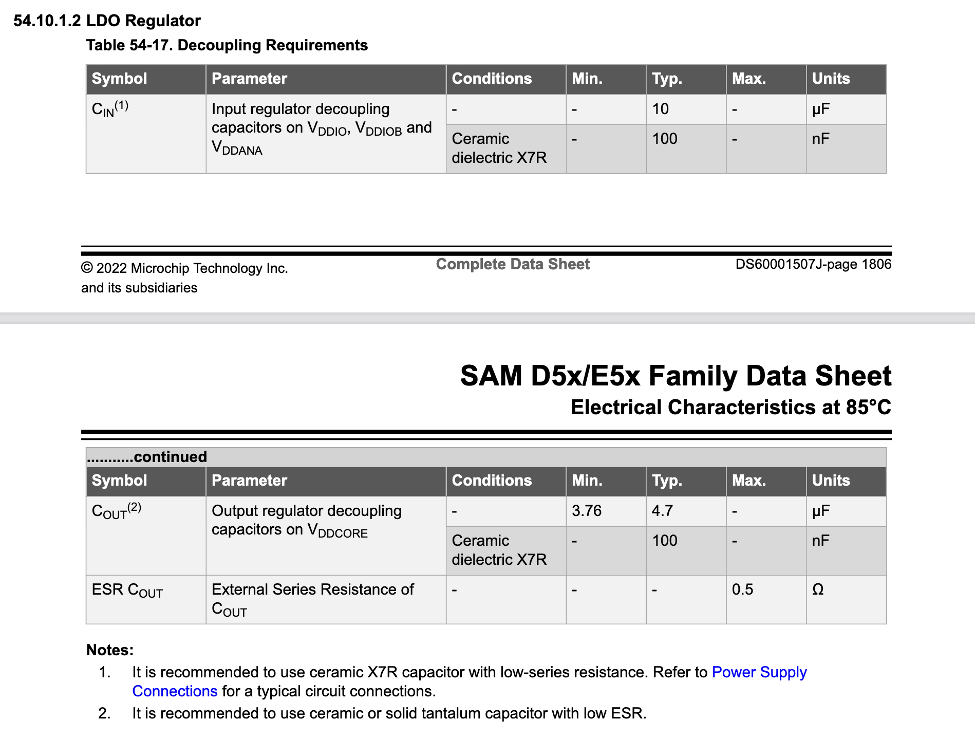
The reason I feel like my 10-pin-to-6-pin cable could work is that only 5 pins are actually needed to program this device, per the diagram in the schematic checklist:
I’ll start from the part library that’s available from tag-connect’s site - then make a new 5-pin schematic for the programming pads, and a new ‘device’ that provides the mapping from the 6-pin PCB footprint to the 5 pins that I need in the schematic:
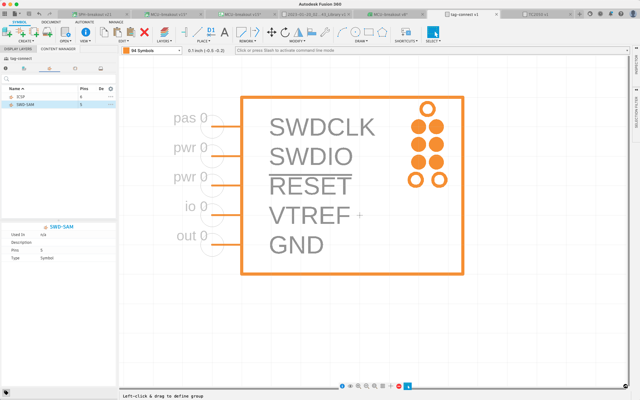
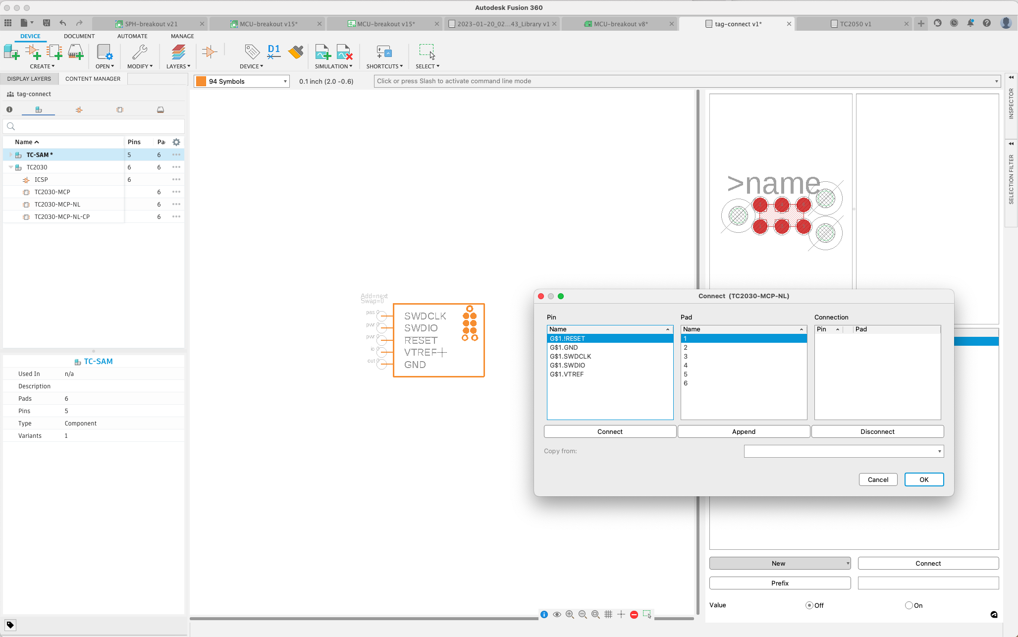
The meat of the process will be in this screen, where I work out the connections from the part schematic to the physical pads in the footprint:
It’s hard to read in that image, but the layout of the tag-connect pins on the PCB is:
| 2 | 4 | 6 |
| 1 | 3 | 5 |
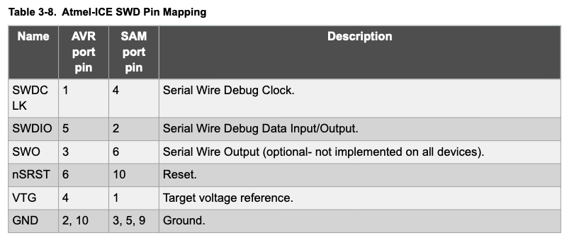
I have the following to work on from the programmer’s user guide - the pins used for SWD programming of SAM ARM devices:
And a working component I’ve used before to program AVR devices from an ATMEL-ICE, using the same adapter:
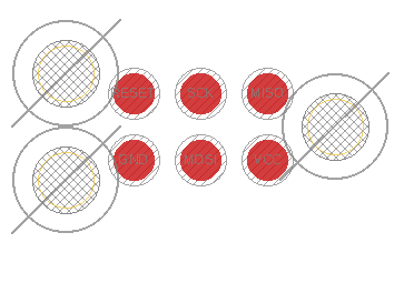
This - if I rotate it around in my head - has the layout on AVR programming signals of:
| VCC | MOSI | GND |
| MISO | SCK | RESET |
Which corresponds to AVR-port ATMEL-ICE pins of:
| 4 | 9 | 2 |
| 3 | 1 | 6 |
Which should correspond to SAM-port ATMEL-ICE pins of:
| 1 | X | 3,5,9 |
| 6 | 4 | 10 |
It’s possible this cable doesn’t work for me - I need pin 2 of the SAM header for data, which is AVR-port pin 5, and judging by the fact that AVR programming uses all 6 pins on this adapter cable, and none of them connect to AVR port 5 (it’s unused in SPI programming of AVR devices), I think it’s one of the header pins not plumbed through to the pogo pins. Ugh. So maybe no need to bother with the multimeter. Judging by the product page for the cable it doesn’t mention SWD programming either, so, blech. I should have started there!
Actually, looking at their site, they have a specific cable for programming Cortex devices with SWD for $42.95. This seems like a not unreasonable tool to add to my toolbox - I’m sure in the future I’ll be using more advanced MCUs like this. And it has its own datasheet which gives specific pinouts for the footprint - which will mean I can finish making this new component in EAGLE and move on.
With that adventure out of the way - and a 1k pullup on the programming clock signal as recommended in figure 60-13 in the datasheet - we’ve got our programming interface set up:
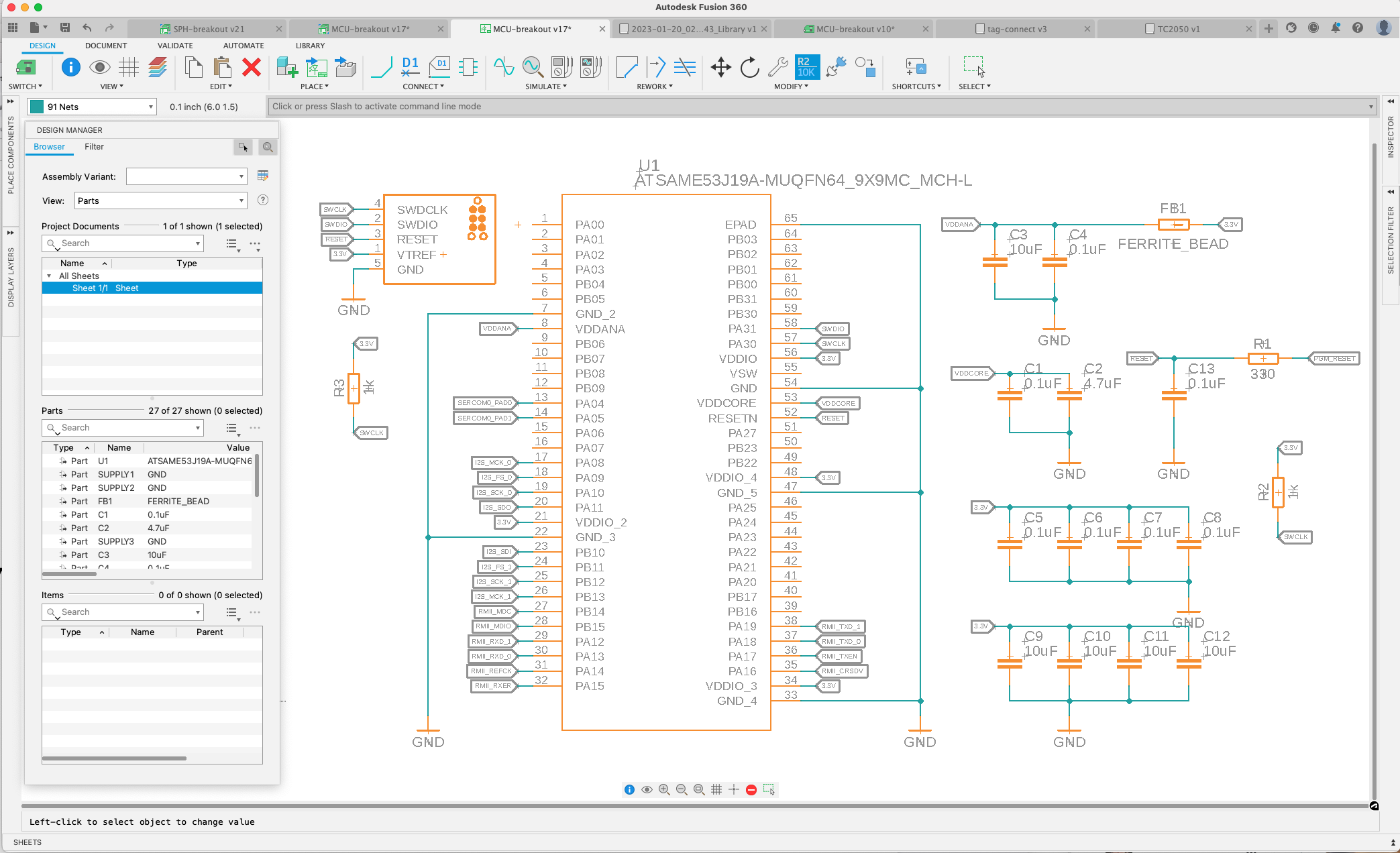
A keen eye will notice that the programming pins overlap with the SERCOM 7 IOSET 1 pins we’d chosen for serial debug. I switched them over to SERCOM0 IOSET 3 for which I wasn’t using those pins for anything else.
PCB Power / Conclusion
As mentioned above - I hope to be able to hook this up to a PoE breakout later, so for now I’ll assume I’ll find a 3.3V voltage source from somewhere else, and just put in a couple of header pins for 3.3V and GND.
I think I’m going to stop there - this schematic isn’t near done though. What it needs next - which will be either Part 6 or Part 7 depending on when I can get to assembly of the I2S breakout - is the ethernet PHY and RJ45 jack, as well as breakout headers for the I2S signals, ideally ones that the microphone breakout board can just plug right into. I’ll also probably then look at the layout and just add breakout pins for every other I/O signal that looks easy to route, since that’ll maximize the future use of this as a general-purpose microcontroller test platform for later projects.
Re-reading this post through - I actually found that I’d made a potentially costly mistake! I’d created a PGM_RESET net earlier when making my reset circuit, but when I added my programming header, I called it RESET. Great example of the easy ways to mess this up.
Cost Update
Since we had to order that new cable, I’ve added a ‘tools’ row to this table:
| PCBs | $2.70 |
| Stencils | $14.74 |
| Parts | $16.71 |
| Tools | $52.95 |
| Total | $87.10 |
At least that cable will be re-usable forever in other projects!