The First PCB Mistake
All of the needed components, the PCBs and the solder paste stencil have arrived and I’m ready to put these together:
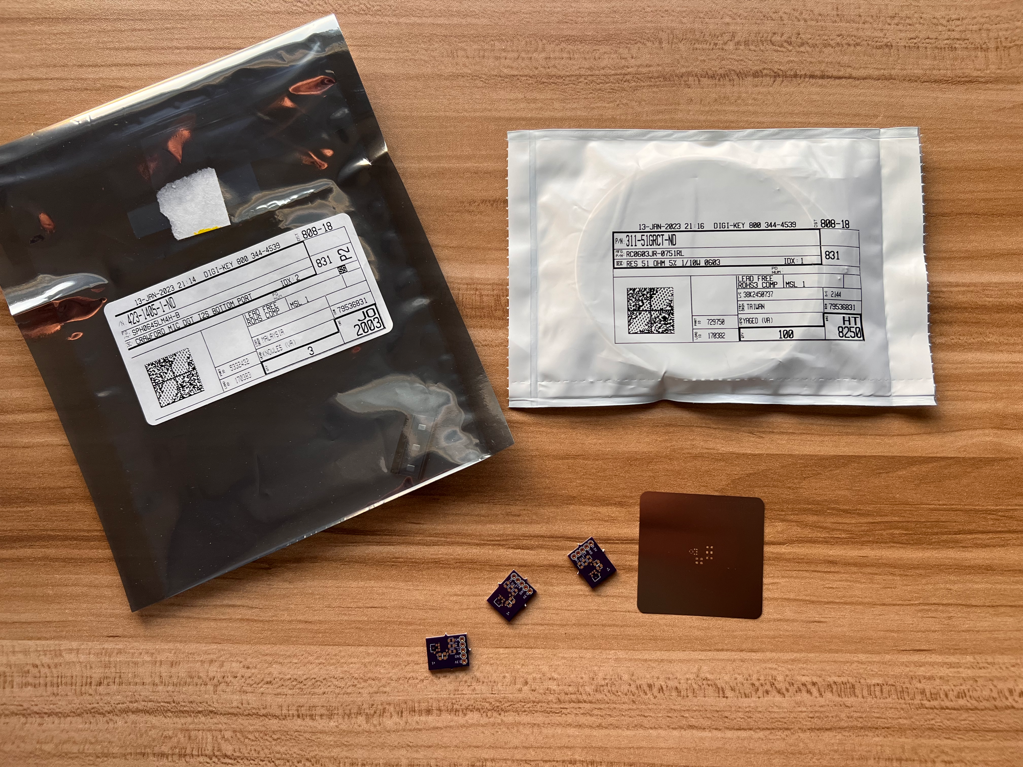
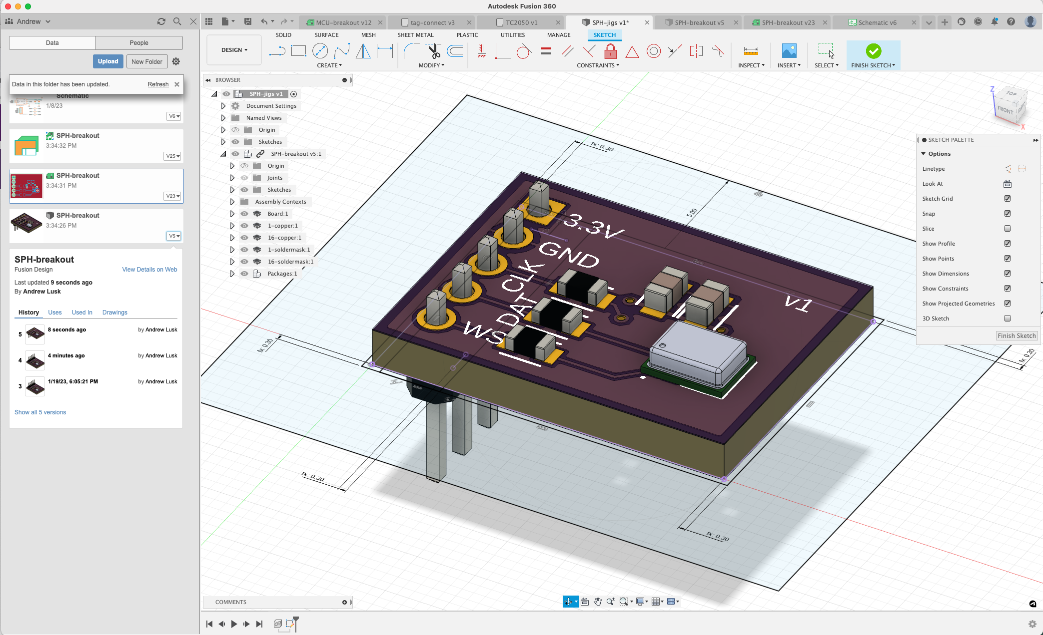
Something doesn’t look right, though…what’s wrong with this picture?
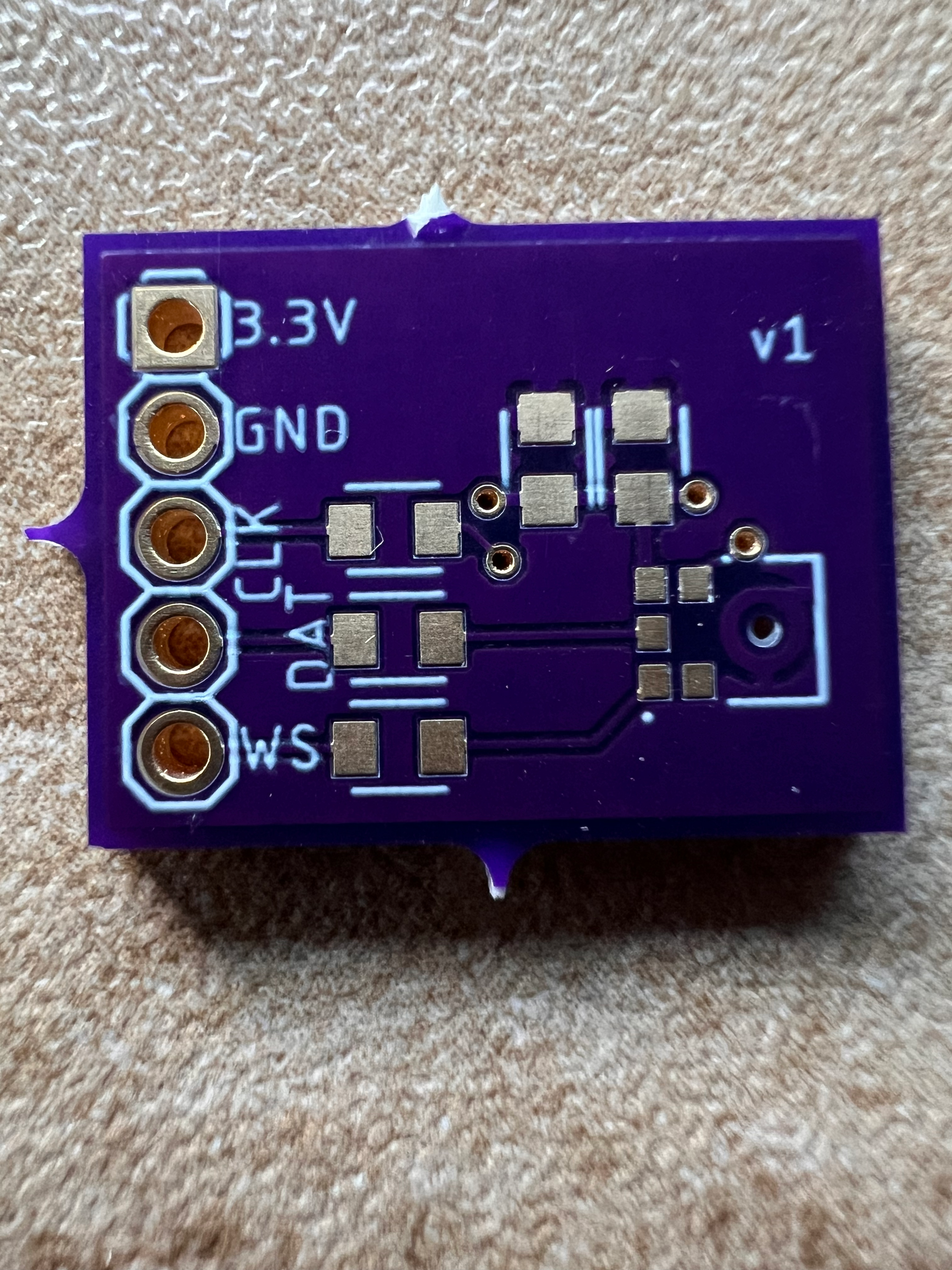
Where’s our ground pad that’s meant to be in a ring around the drilled port for the microphone? I see the copper there, but it’s got soldermask over it.
Crud. Checking my OSHPark order history - the PCB preview images show the same issue, so the fact I ordered these is decidedly sloppiness on my part - I should have caught it then.
What could be causing this though? I downloaded the part online - I didn’t make it myself. Often this works great, but still in this case it’s the first place I look. I open up the footprint in Fusion:
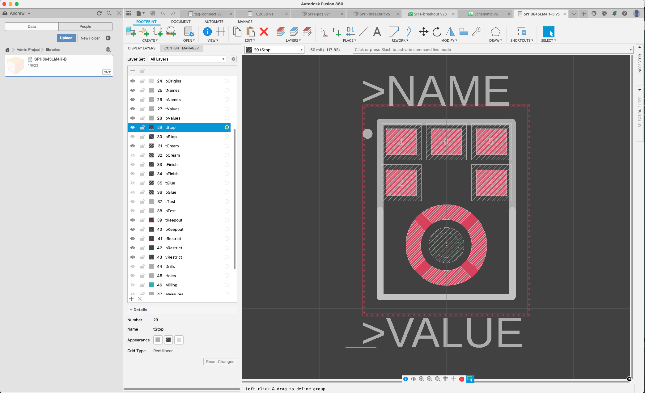
This appears right at first glance…it even has the gaps in the ring meant to limit the amount of solder paste dispensed (often for big ICs with a big ground pad you’ll see a cross-hatch pattern in solder stencils, for this same reason).
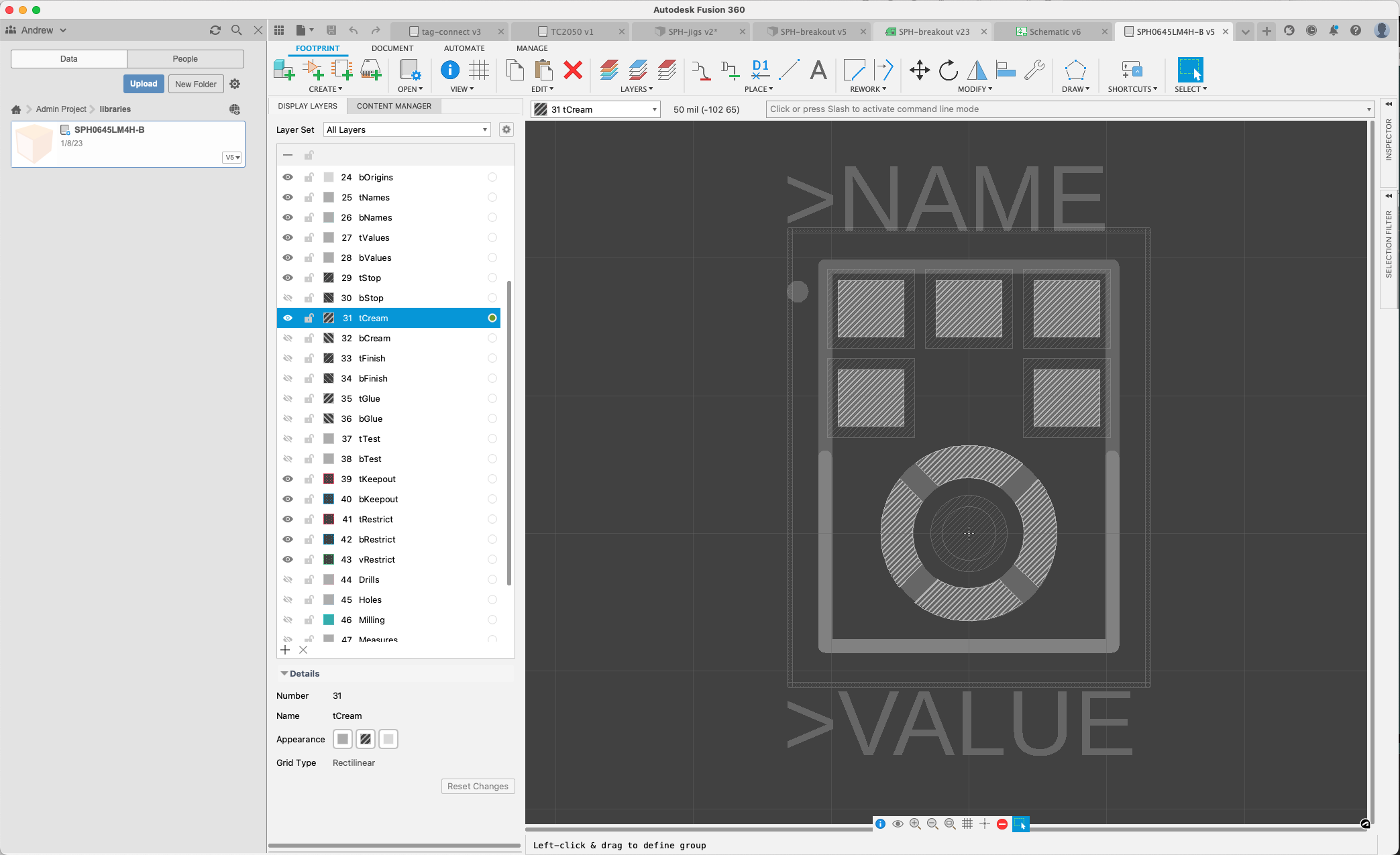
Looking layer-by-layer, the ‘tCream’ layer which is used by OSHStencils to manufacture the stencil (which looks just fine), has these:
But the ‘tStop’ layer, which OSHPark uses to set where the purple solder mask goes, and which should cover at least every pad that’s meant to be soldered to, has nothing around the ring! This is hard to see in screenshots where you can’t see the UI transitions between layers - but the top 5 square pads have a highlighted outer square here.
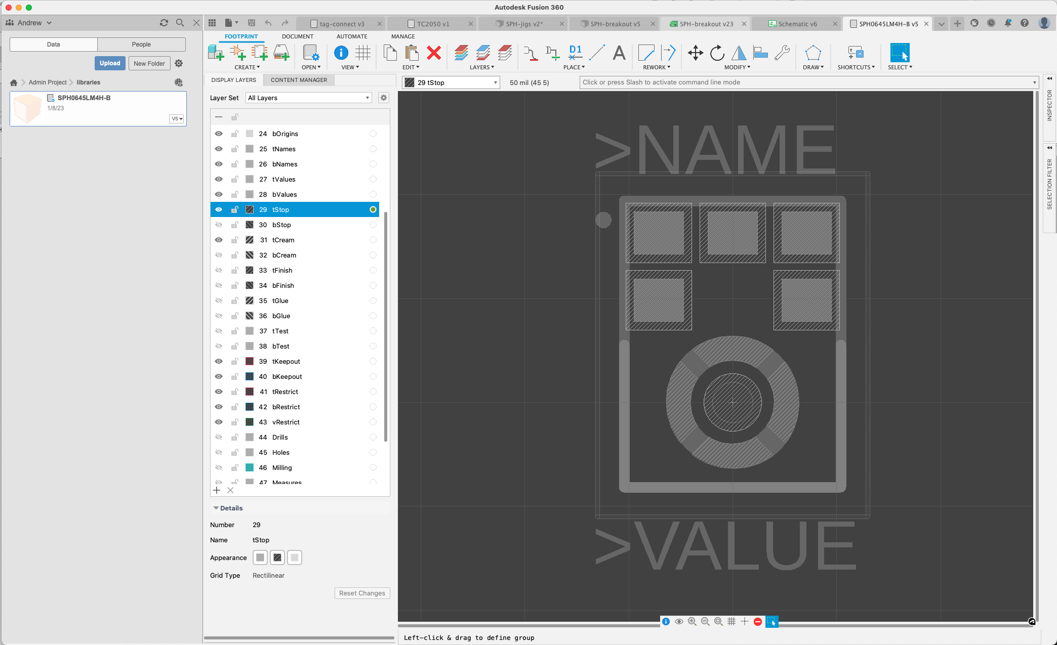
It has a circle around the actual drilled hole, but not the pads surrounding it. Whoops. Not hard to add one in, that just covers it all:
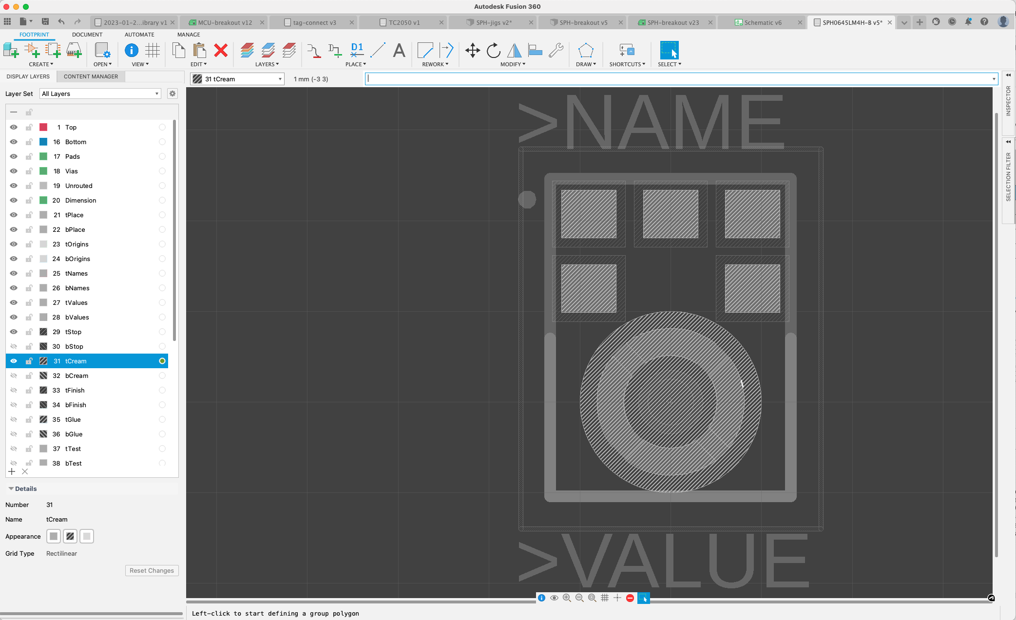
I lied - it was a little hard, as what Fusion really wants you to do is just lay out surface-mount pads and let it automatically create the tStop (top-layer solder mask) and tCream (top-layer solder paste dispense) layers from the dimensions of those pads. But it also doesn’t support non-standard-shaped pads. Digging in, the way this ring-shaped pad was created was by actually making one small square pad, then drawing a custom polygon on the top layer in the right shape. The UI also doesn’t allow for easy arbitrary drawing; I had to break out the command line to draw a ‘CIRCLE 0 (0 0) (1 0)’ to make a 1mm-radius circle in the tStop layer (this was after being confused for a while accidentally creating it in the tCream layer, which you can see in the screenshot above is the one I have currently selected. Oops).
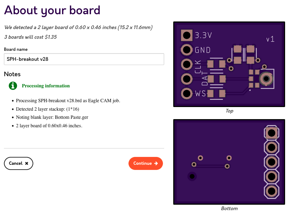
Anyway - now OSHPark shows a break in the solder mask in the board preview:
I forgot to update the ‘v1’ silkscreen to ‘v2’, but given I’m pitching the useless ones I have, and the new ones are pretty visually distinct anyway, I’m not worrying about it.
Since nothing’s changing about the physical dimensions of these PCBs, I’m actually going to take the time to go through how I use my 3D printer (a Prusa i3 mk3s, which I heartily recommend as about as plug-and-play as a 3D printer can be) to assist in assembly.
Jigs for stenciling and soldering
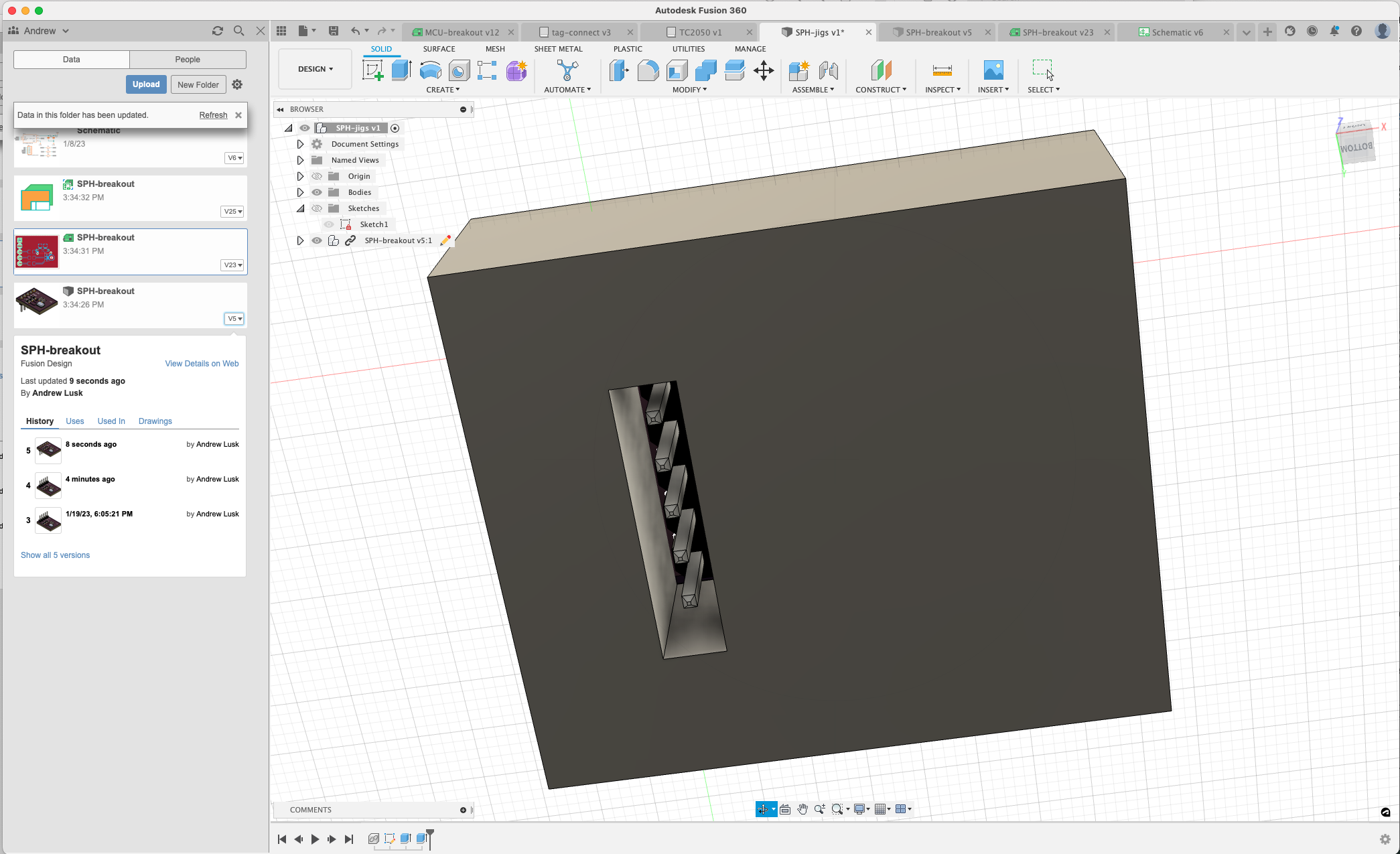
One thing that’s really handy about having both a 3D printer and using a CAD program like Fusion 360 for PCB design is that it’s pretty easy to solve some fiddly assembly problems with little throw-away jigs. I’m actually going to want two for the assembly of this component: one, to help position the 5-pin male header pins so that I can solder them in nice and perpendicular, and another to help affix the much larger solder paste stencil in a way that’s aligned to the board.
The first thing I do is actually go in and flip the header component to the ‘bottom’ of the board. It makes no difference to the PCB layout, because it’s just 5 through-holes, but it positions the pins facing down in the 3D model:
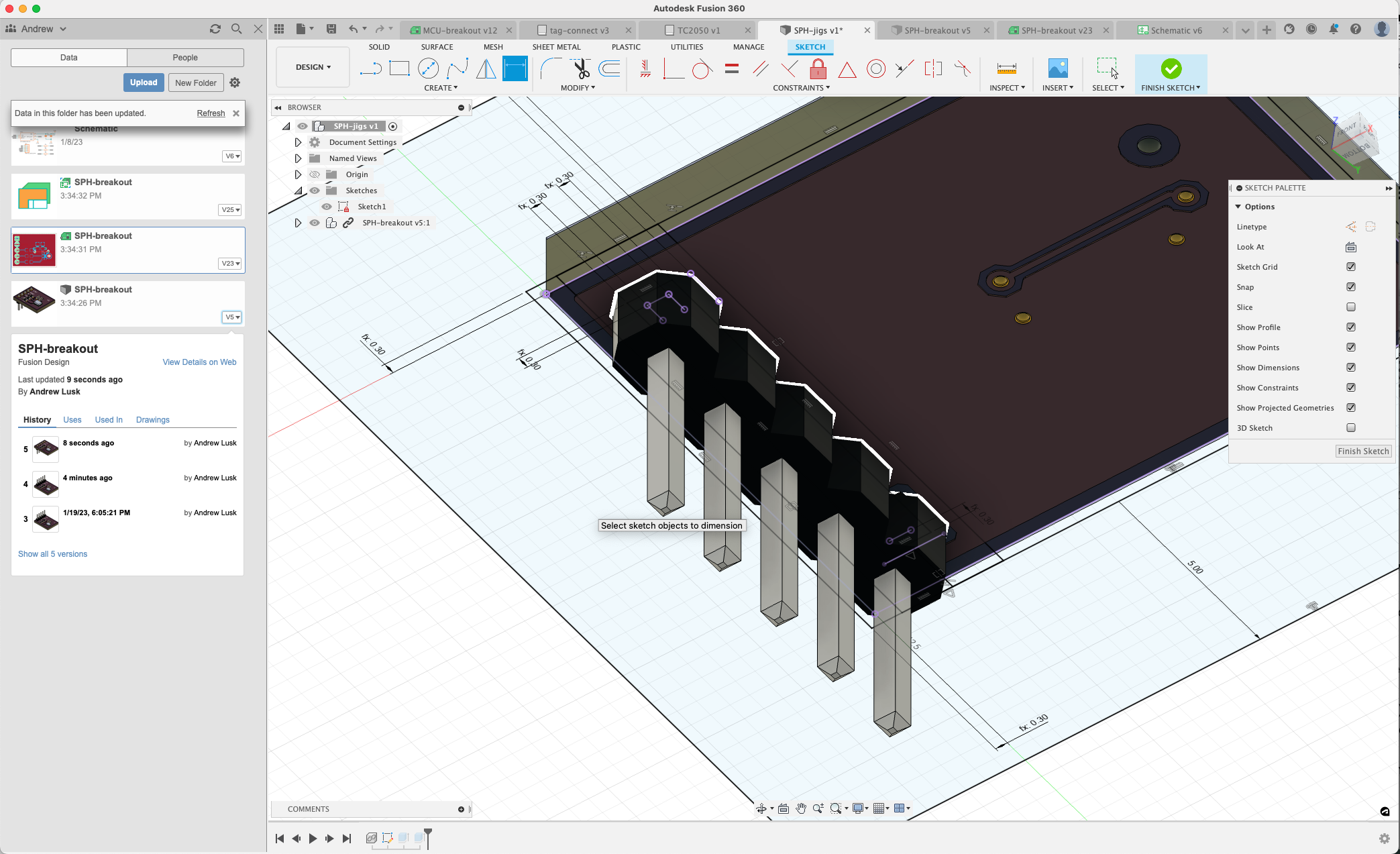
Now I can start building a sketch around this - something I can drop the 5-pin header into, then put the PCB on top, nice and snug so I can easily solder the headers in. BTW, I could do this on a breadboard without too much trouble, but I’m (a) a poor hand-solderer and they usually end up wonky when I do this, and (b) really just trying to show “a neat thing you can do”. 3D printing is going to come in really handy later when, for example, we want to apply solder paste through a stencil onto the back of a PCB that is already populated on the other side. For now, this jig is for funsies.
I define a Fusion “parameter” called “offset”, at 0.3mm which I just then use all over this design as my “buffer space tolerance” value. With the basic sketch in place I can extrude it down around the header:
And then project just the pins into the sketch:
So that I can bring the sides of the cavity closer in for the black plastic parts of the header to sit on:
Now - on to the next one. This is just going to be a border around the PCB that we can sit it in, tape it to on the back, and then with 4 ‘arms’ going out a couple of inches so that the stencil has something to get taped onto also. For bigger PCBs I have a better system that I’ll write about when I do one of those, but this will do for now.
After a quick sketch and extrude:
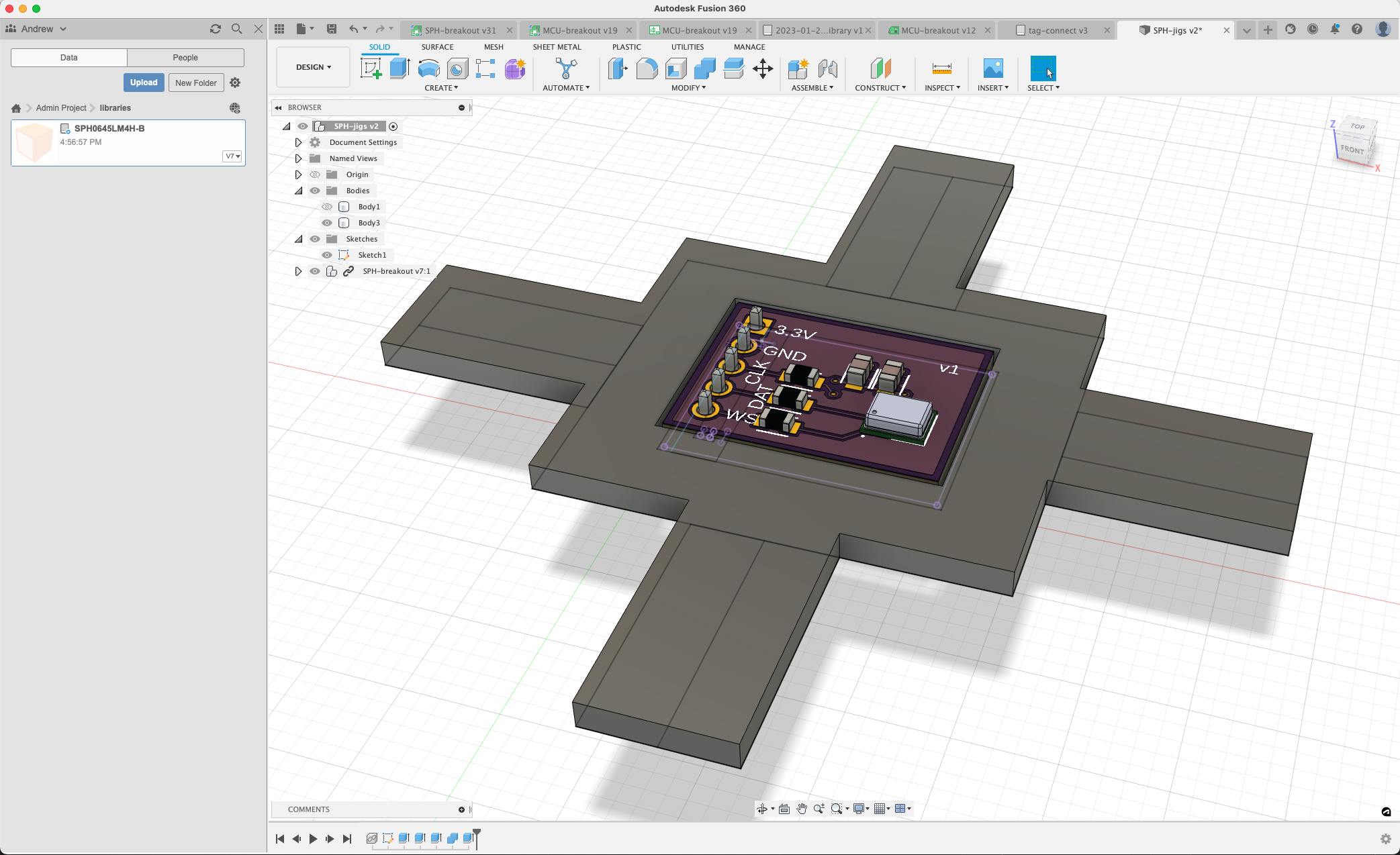
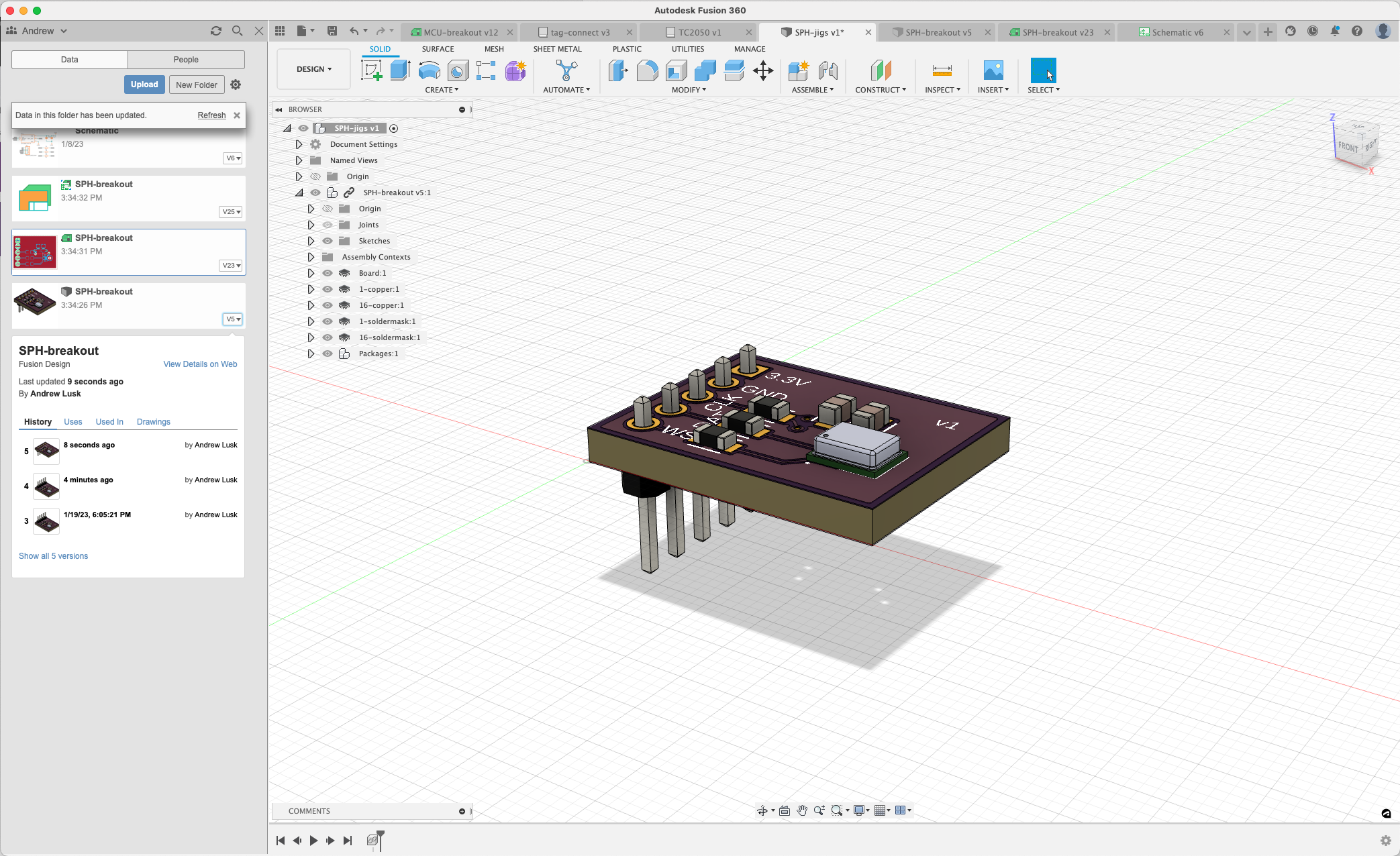
We’ve got a couple of little jigs ready to go:
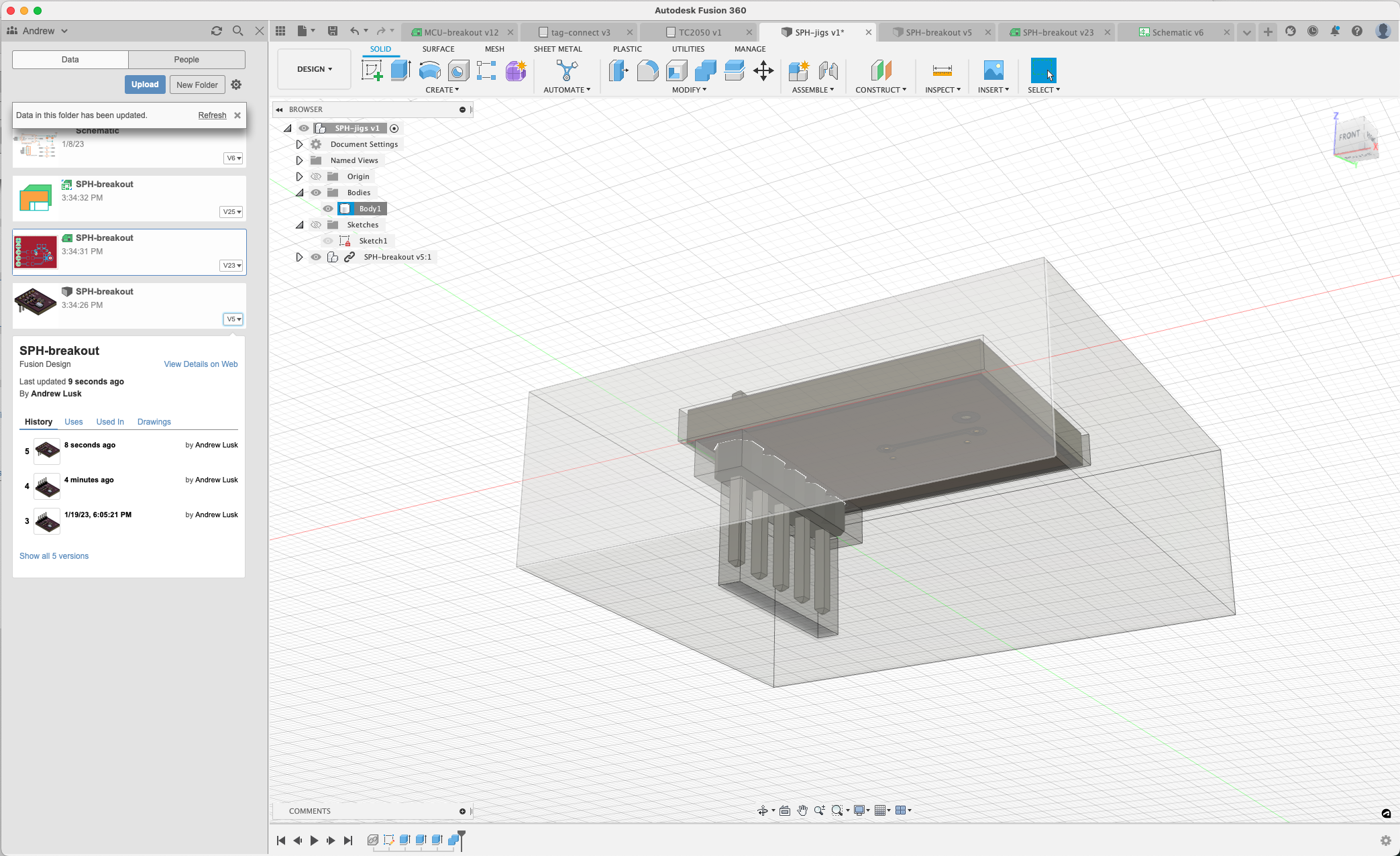
However - I notice three problems. The first two are easy - my ‘offset’ of 0.3mm is a bit generous (I always tend to underestimate how big a millimeter is, and how accurate PCB houses and 3D printers are), and the ‘arms’ on my stencil jig are a bit too short to give me a good taping surface to adhere the stencil to.
The third is a fun one - there’s a gap between the top of the stencil jig and the top of the PCB, which means that solder paste is going to spludge out (techincal term) during application. It turns out that I’ve made two mistakes. One is that Fusion thinks my PCB is thicker than it is. Checking the layer stackup in the “manufacture” tab shows me that it thinks it’s got 1.6mm of substrate before you account for the copper:
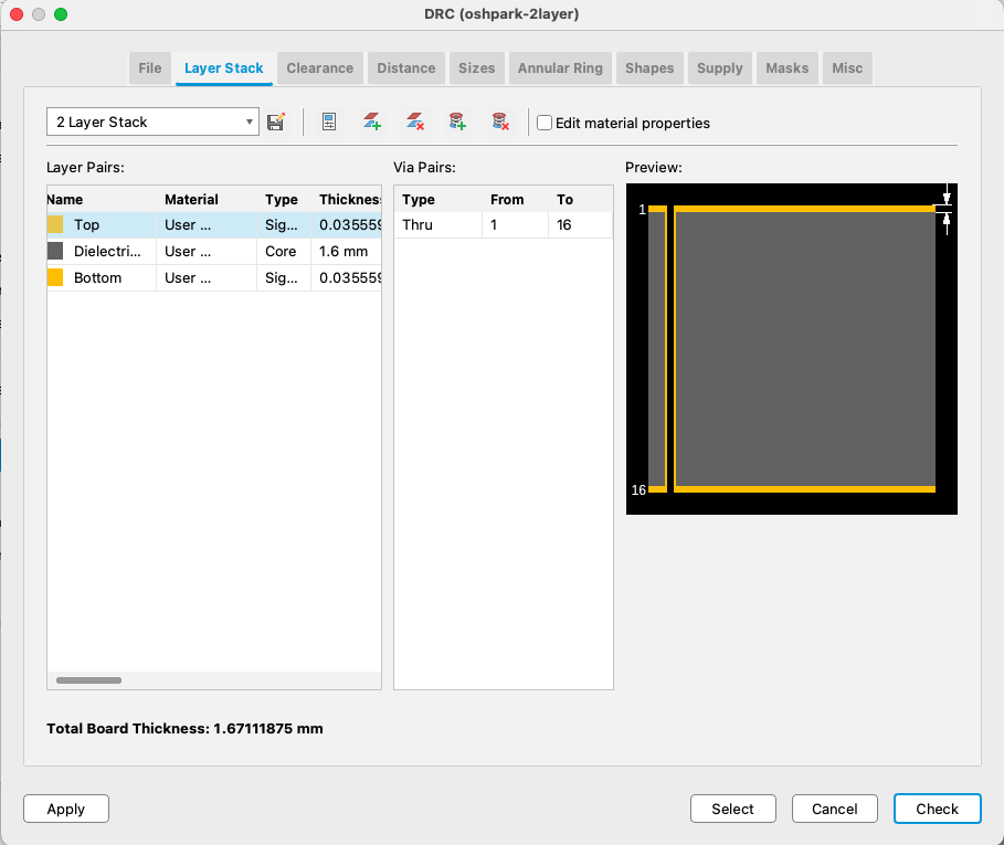
But the official stackup on OSHPark’s site says that the interior substrate is just 1.524mm. So - that’s easily fixed in Fusion.
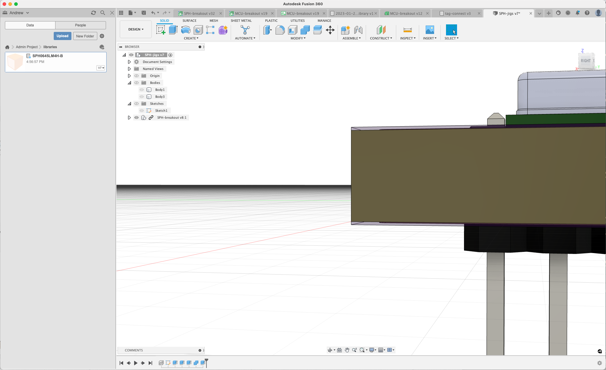
The second mistake I made was that I was extruding the jig body up from the ‘z=0’ plane, but the way that the 3D PCB model was imported was such that the bottom of the substrate was placed at z=0, not the bottom of the PCB, counting the copper plane on the bottom layer. It makes a tiny difference - as you can see below:
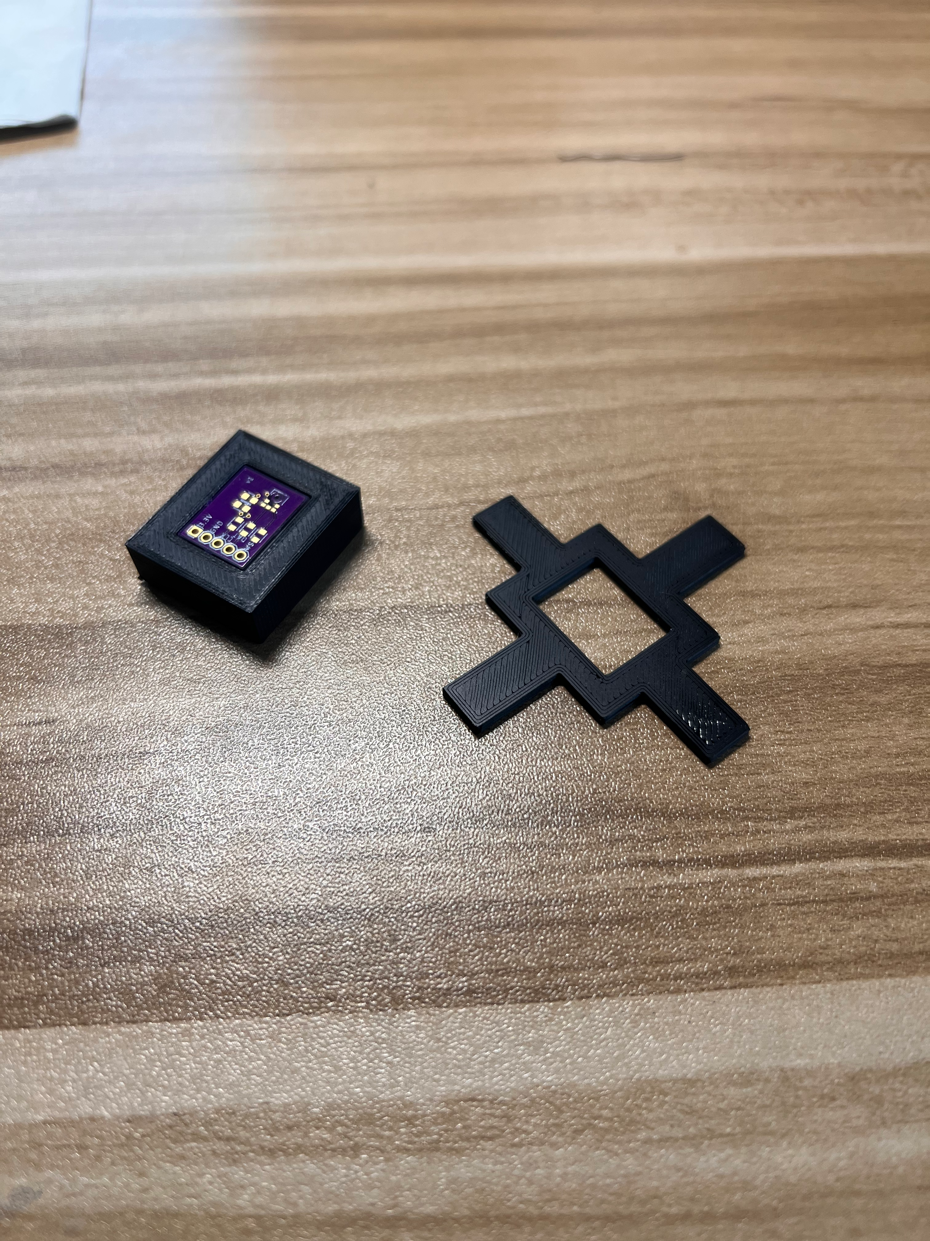
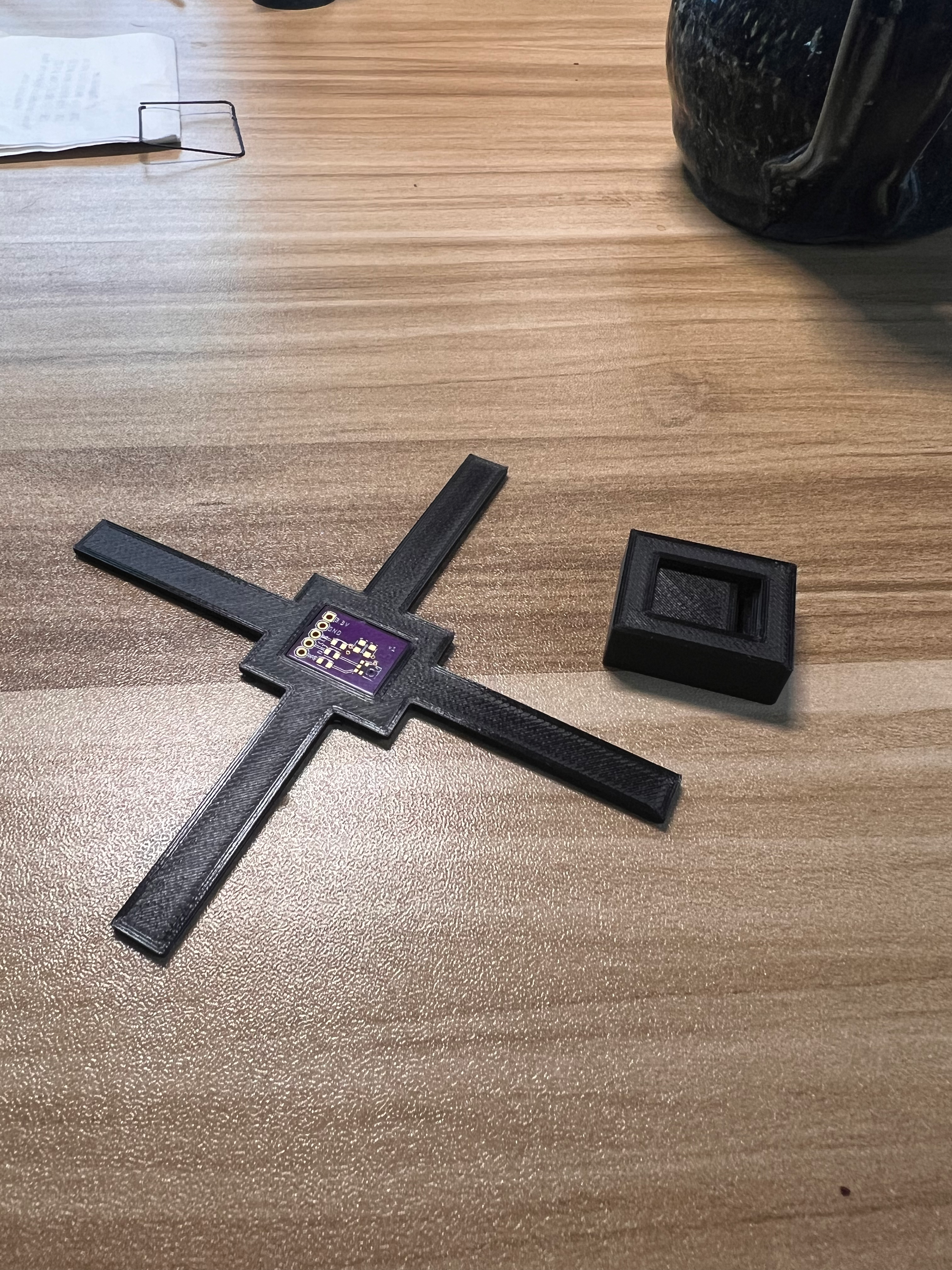
After another round on the printer we have two new jigs that fit the PCB satisfyingly flush and snug:
We’ll leave it there for now. I’ll likely continue Part 5’s efforts on the MCU + Ethernet schematic in the time while I’m waiting for the revised PCBs to arrive.
Cost update
After the botched first round of PCBs, it was another $2.70 to order the fixed ones. Check everything twice!
| PCBs | $5.40 |
| Stencils | $14.74 |
| Parts | $16.71 |
| Tools | $52.95 |
| Total | $89.80 |