Picking up where I left off in Part 5, I’m going to continue to add components to the schematic for the MCU breakout board. My goals are to get the ethernet PHY and RJ45 jack added, and then add some external connections for serial debug, power, I2S, and maybe just a few other I/Os if space permits. Maybe a test LED or two also.
MCU Clock
I did some more digging on whether I really really could get by without an external crystal for this MCU’s clock. I found that Microchip actually has a quite handy sort of “starter template” web tool, where you select and configure the peripherals you’ll use, as well as the MCU itself, and it’ll give you a starting code base to work from. This includes clock configuration, and being able to play around with a visual tool for clocking helped me understand better why I might want an external crystal - I’ll definitely need one if I want to run at anything higher than the 48MHz that the internal clock source can do, up to the CPU’s maximum rating of 120MHz. I’m actually hoping 48MHz will be fine.
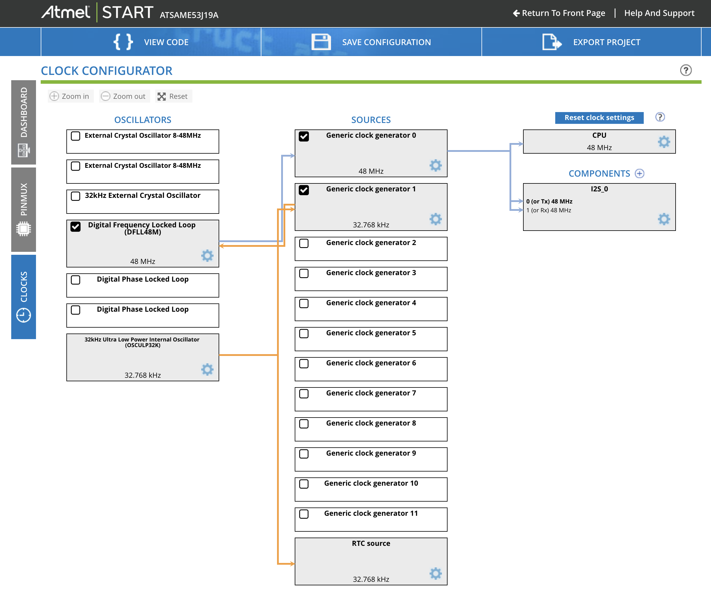
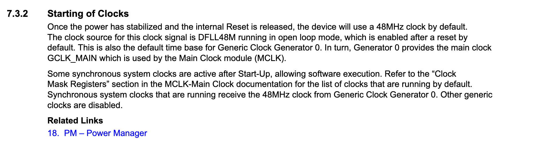
The tools lets you know if you’ve picked an invalid configuration; I was able to get this all logically connected together with what appears to be no errors or warnings, so I’m increasingly convinced I’ll be fine. Looking in the datasheet - it’s actually also explicitly called out that, until the MCU is explicitly configured to do otherwise, it starts up at 48MHz coming from the internal PLL:
So - moving on for now to the PHY.
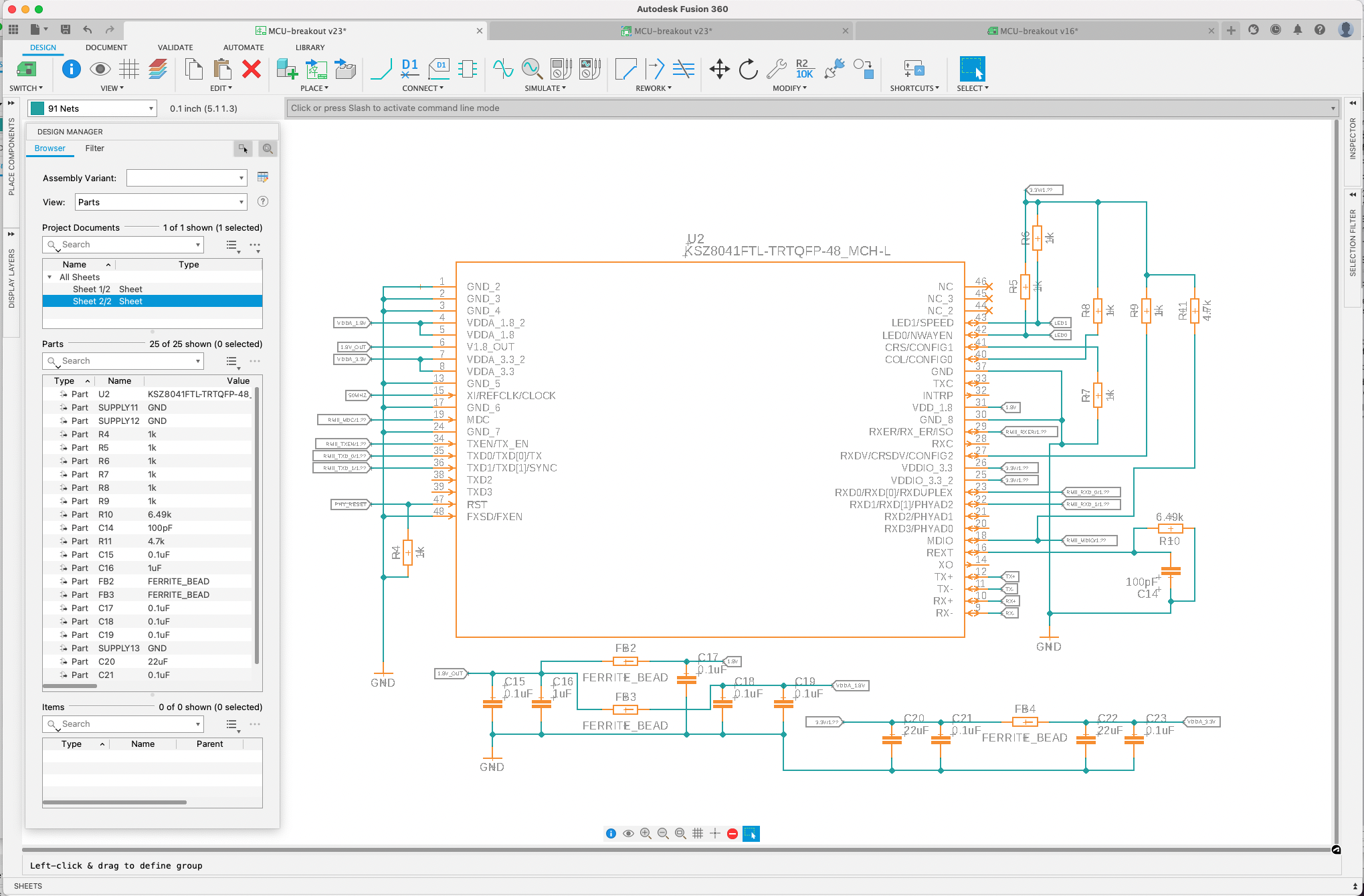
KSZ8041 PHY Schematic
I swing by Microchip’s website to download a library file for this part:
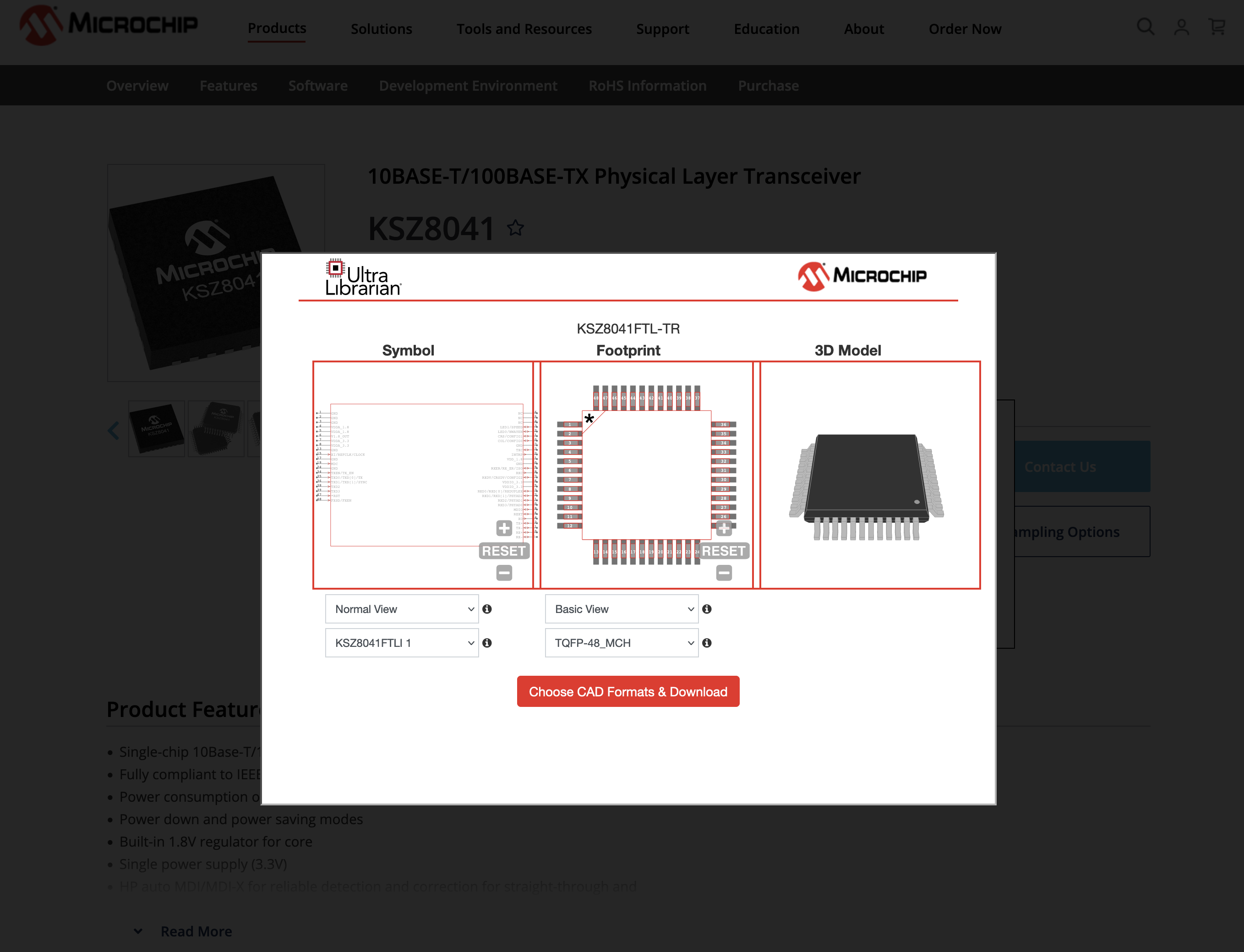
And then import that into my MCU breakout schematic - I do this on a new ‘Sheet’ of the schematic, which gives me a blank canvas to work on. I like to use one sheet per major component (I’ve rarely had more than 2 in any case). This one looks even more intimidating than the MCU!
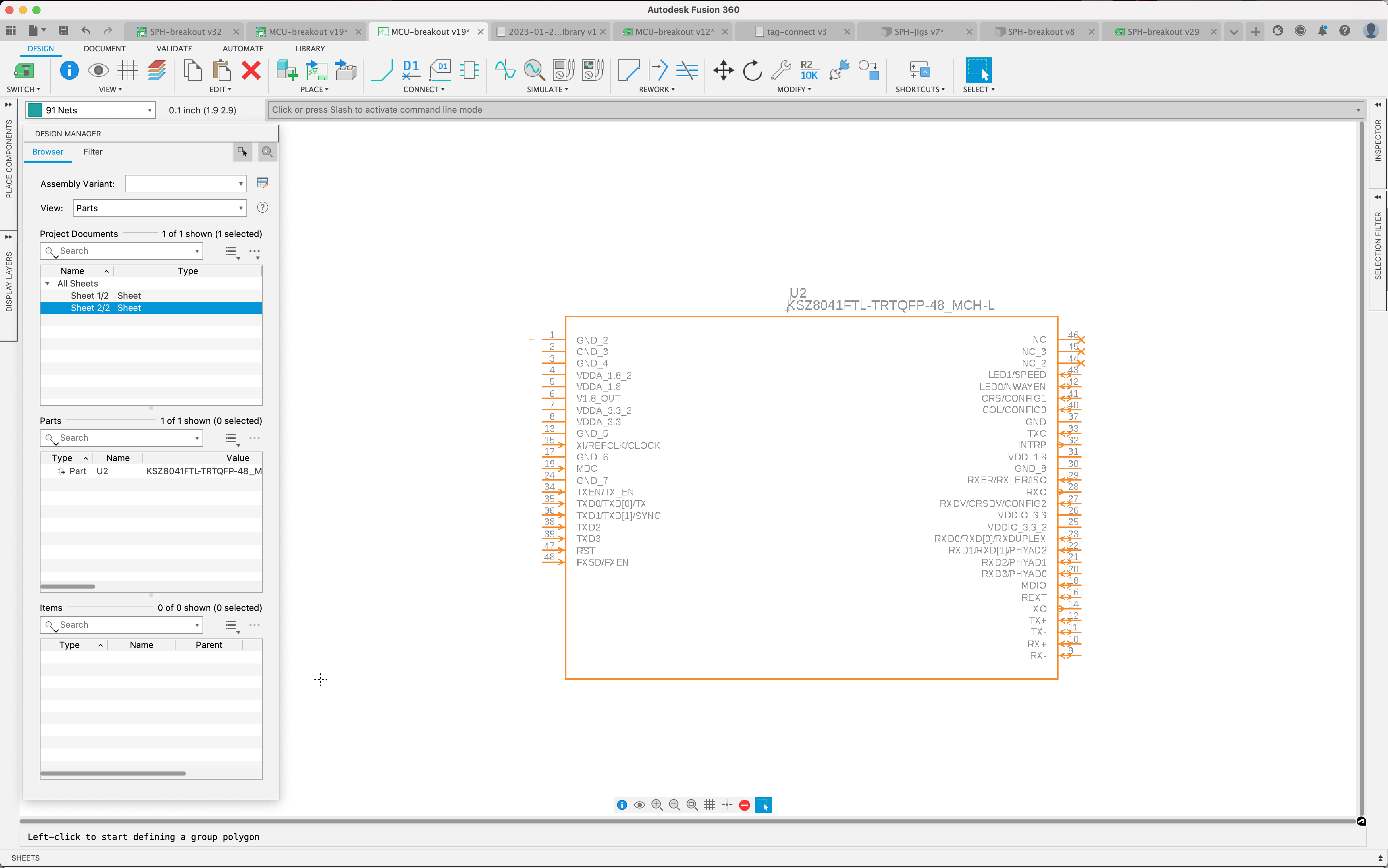
But - I think it’ll be OK once we start walking down the datasheet. I start walking down Table 2-1 which lists out the signals pin-by-pin.
- 8 pins for GND.
- 2 pins each for analog 1.8v and analog 3.3v inputs.
After this I’m down from 48 to 36 pins left:
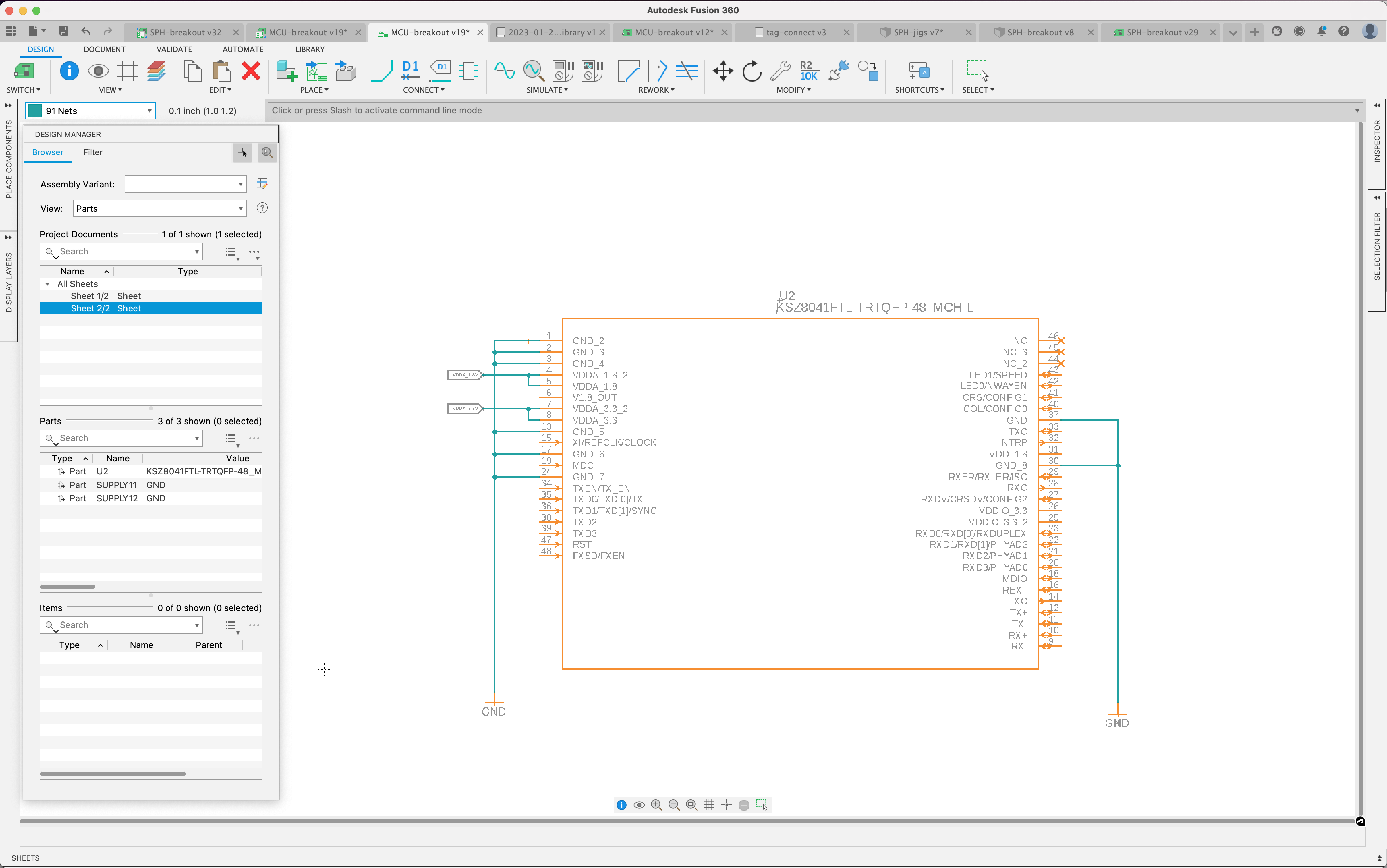
Working my way down the left side of the schematic (for no particular reason other than how it looks):
- Added a 50MHz net to hook up the oscillator when I get that part placed.
- Connected 4 of the RMII lines - the command clock and three TX signals.
- Left 2 MII-specific pins not connected.
- Added a PHY_RESET net that will be controlled by a GPIO on the MCU, with a 1kΩ pull-down resistor to hold it in reset until I’m ready.
- Connected the fiber-detect pin to GND, per the datasheet, to indicate to the PHY that we’re in copper mode.
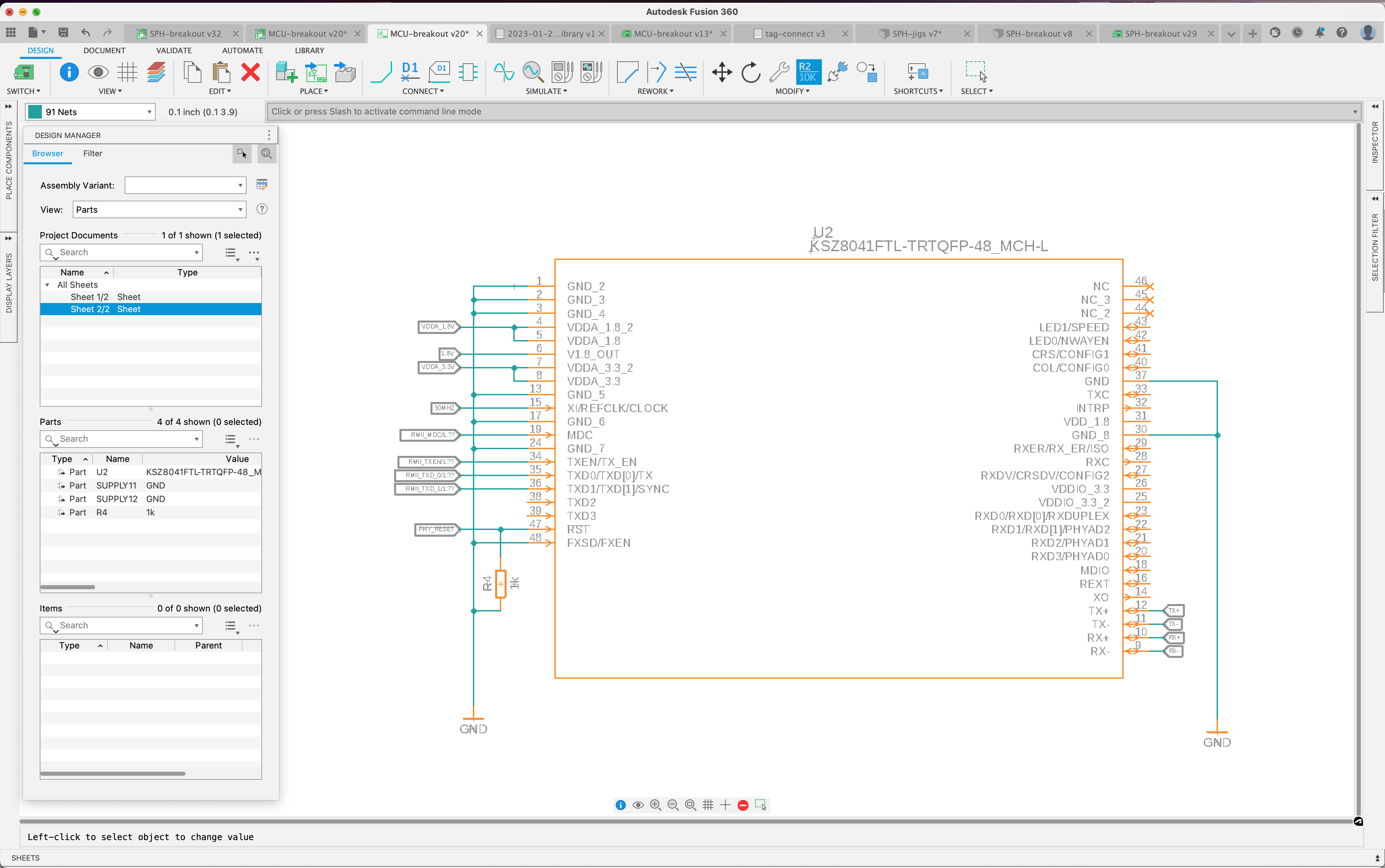
THen walking down the right side:
- I get to leave the first 3 pins unconnected.
- The next pins - for the LEDs on the RJ45 jack - work like a few other odd ones do on this part, which is that they’re actually doing double-duty as configuration inputs to the IC when it comes out of RESET. So - for LED1/SPEED I add a pull-up to configure 100MBit, and for LED0/NWAYEN I add a pull-up to configure auto-negotiation.
- CONFIG0/CONFIG1/CONFIG2 are what we use to tell the PHY we’re going to use RMII, not MII. They need to be [2:0] = 001, so CONFIG0 gets a pull-up and the others get pull-downs.
- TXC/RXC are MII-specific outputs.
- REXT requires a specific little circuit to be connected to GND - a 6.49kΩ resistor and a 100pF capacitor to be connected in parallel to GND.
- MDIO needs a 4.7kΩ pull-up.
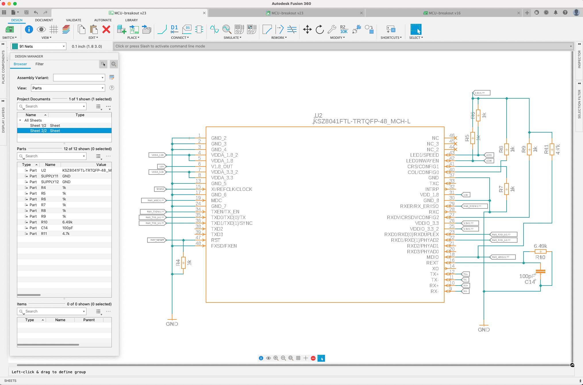
Now I should just have remaining to do all the bypass capacitors and the 50MHz oscillator. There’s a useful datasheet section telling us exactly what it needs as far as power supply bypass:
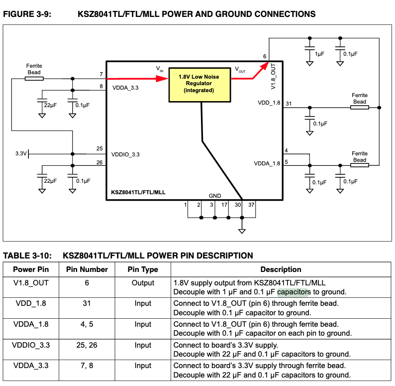
So that’s 1uF and 0.1uF on the 1.8V regulator output, a 0.1uF on each 1.8V input, and a 22uF and 0.1uF on each 3.3V input, with ferrite beads between the digital and analog nets, per the diagram:
Now for the oscillator - I don’t have a 50MHz oscillator lying around, so let’s go to Digikey to find one. Going to Crystals, Oscillators, Resonators -> Oscillators and hitting ‘50MHz’ ‘Active’ and ‘In Stock’ we get 4,014 results. That’s … too much choice. Further narrowing down by “Surface Mount”, “4-SMD, No Lead” (simplest package), and a 3.3V supply, we’re down to 638 options. I think at this point I’m just going to go with the first result:
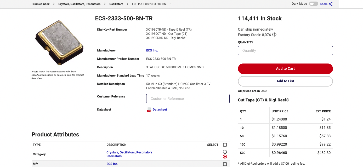
As it’s pretty reasonably priced and has plenty in stock. This oscillator’s Datasheet looks like it has everything we need, including letting us know in the “land pattern” section that it wants a 0.01uF-0.1uF bypass capacitor between its own VDD and GND pins. It also looks like there’s a symbol and 3D package available from SnapEDA for this part.
RJ45 Jack
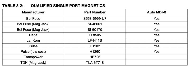
With that we should be done with the PHY…but we still need an actual ethernet port to connect it to. I also don’t have any of those lying around, but the nice thing is that the datasheet helps with a list of jacks that have integrated “magnetics” (which are, handwave handwave, some important component of the very analog physical interface that is ethernet cable).
Let’s check Digikey for these…they have just 135 in stock that are single-port, no weirdness like USB, in the ‘Modular Connector Jacks With Magnetics’ category.
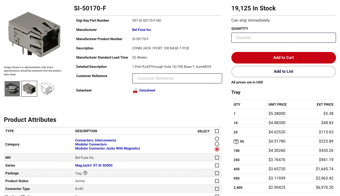
But then when I narrow further, I can see the SI-50170 is in stock for $5.38:
So this seems like an obvious choice - let’s download the model from Ultra Librarian (linked from Digikey) and import it into a new ‘sheet’ in our schematic, which we’ll use for external connections:
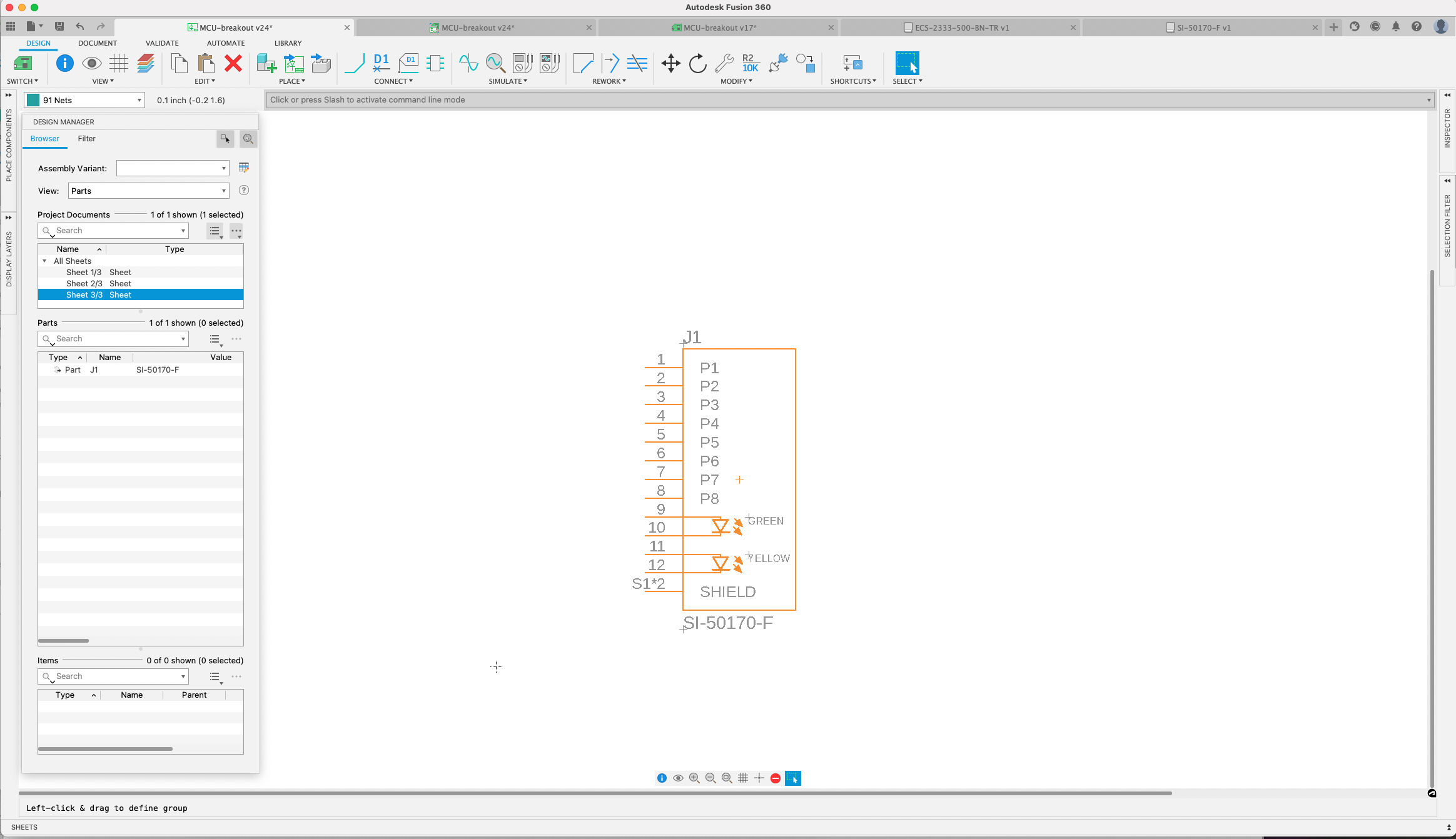
The Datasheet for the RJ45 connector is neat to see; it shows that there’s more going on inside this jack than meets the eye (also that Pin 7 is NC inside the jack).
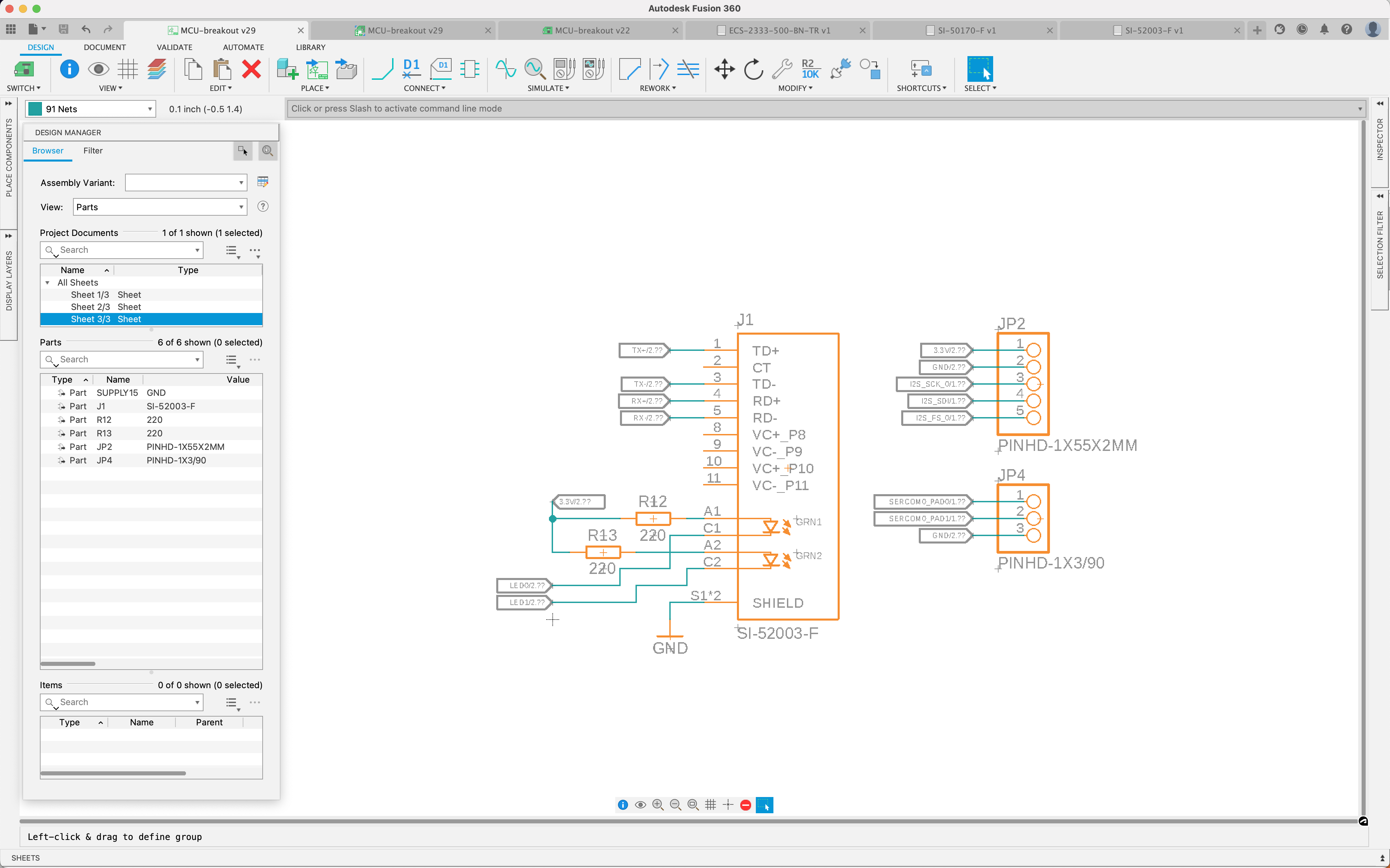
It looks like Pins 4 and 6 are our RX+/- differential pair, and pins 1 and 3 are our TX+/- pair. But wait - thinking ahead to PoE, there’s a challenge here. PoE sourcing equipment has the option to use either the ‘center taps’ of the RX/TX differential pairs, which are broken out here on pins 2 and 5, but they might also use the “spare pairs”, the 5+6 or 7+8 twisted pairs. Those are not broken out on this jack. What I’m going to do instead is go back to my Digikey search, and find another MagJack by the same manufacturer which calls out PoE support explicitly, the SI-52003-F. This datasheet tells us that it breaks out all the pins, so this is really the one to use. Glad I checked!
Additional Headers
Let’s also add in some connections for the link and activity LEDs, so we can be fancy. I’ll put in some 220Ω resistors on those lines (it doesn’t matter if it’s ‘in front of’ or ‘behind’ the LED, just that it limits the current to about 15mA, which is typical for a small LED, and I have a bunch of 220Ω resistors lying around).
And lastly we can add a header that we’ll use to provide RX/TX serial debug to the SERCOM0 pins. This header has a GND reference on it as well, which is a sort of best-practice thing to have when hooking up a totally separate device (one my my USB<->serial converters) where you want to make sure they’re sharing a ground.
I want to come back and add more connections for GPIO, but after the bulk of the physical layout is done, which I’ll get started in the next post. I expect this to be a pretty challenging physical layout, unlike the simple microphone breakout, because we’re dealing with high-speed signals and differential pairs, as well as analog signaling. Both of those are slightly outside of my current comfort zone, so, fingers crossed.