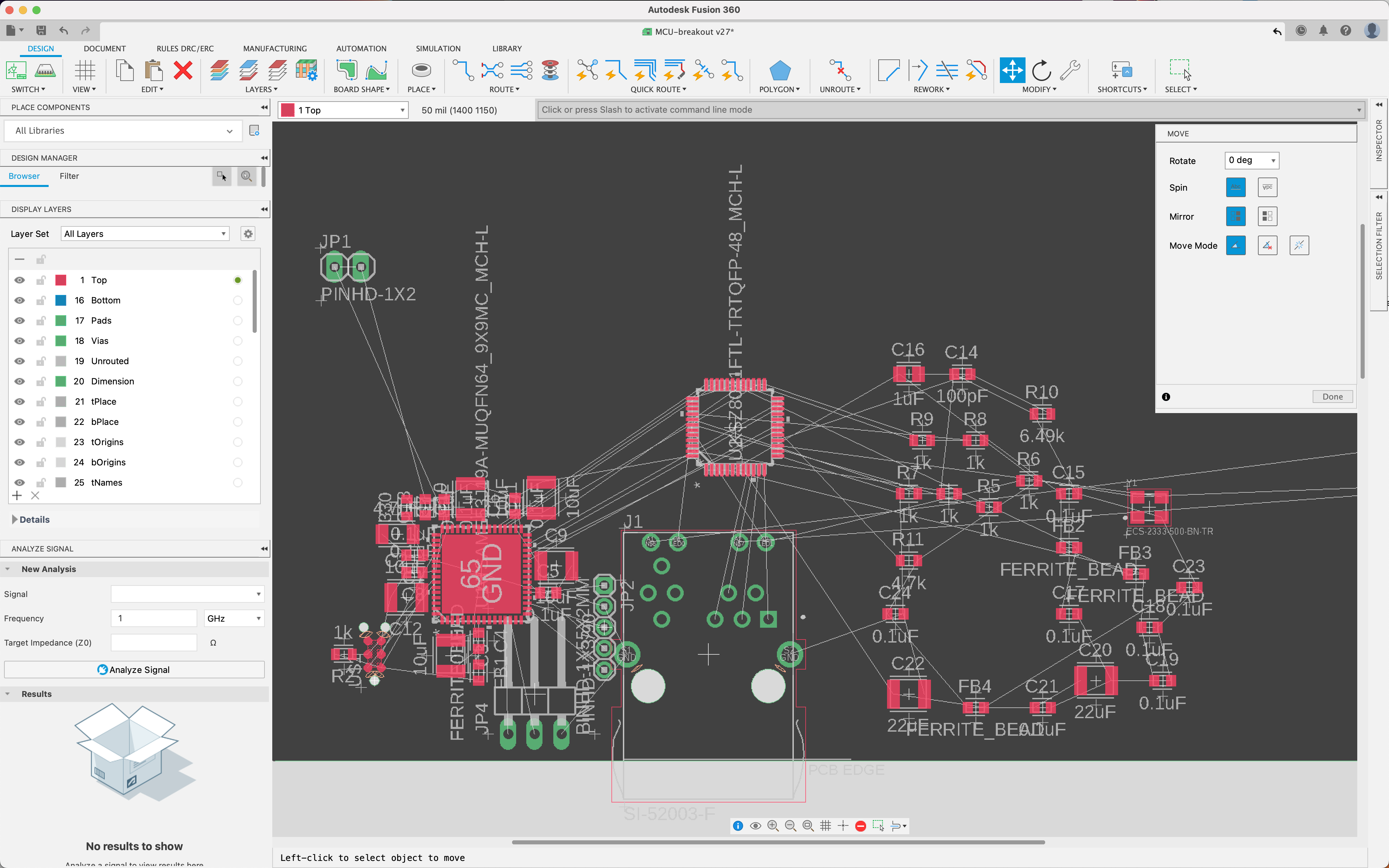
Early Layout
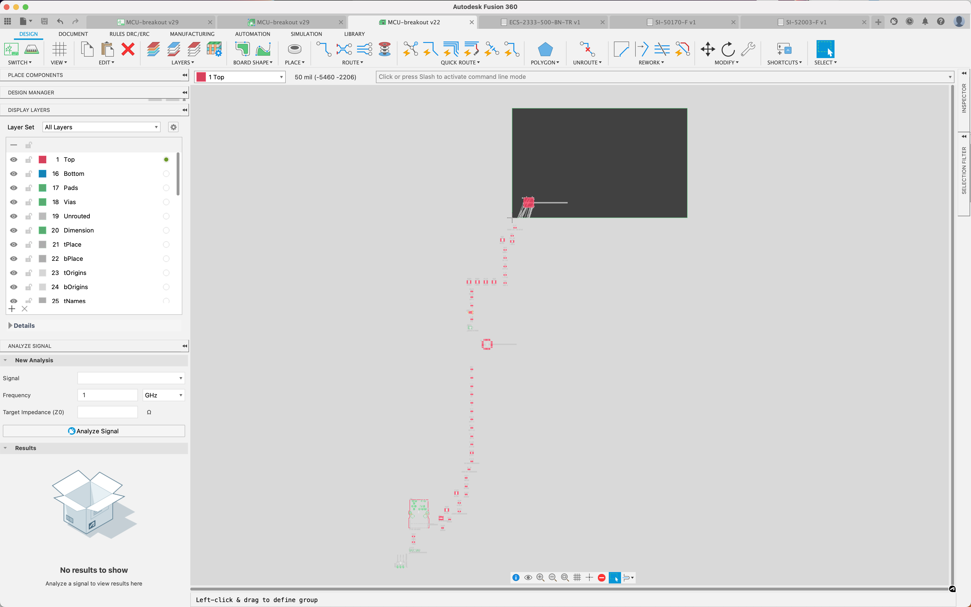
Switching over to the PCB tab after a bunch of time in the schematic is always a bit of an initial fright, since it just lays things out in a giant line:
But this isn’t too hard to corral into a rough shape. Generally my first step is to just fling things into various corners of the board and try to keep passives near the component they’re supporting. What can make this tough is that there are a ton of, for example, 0.1uF 3.3V->GND decoupling capacitors in this design, and some are attached to the MCU and some to the PHY. Luckily, since we did this all in order, with all the MCU components first, we can start off by just using the order in the line as a likely grouping:
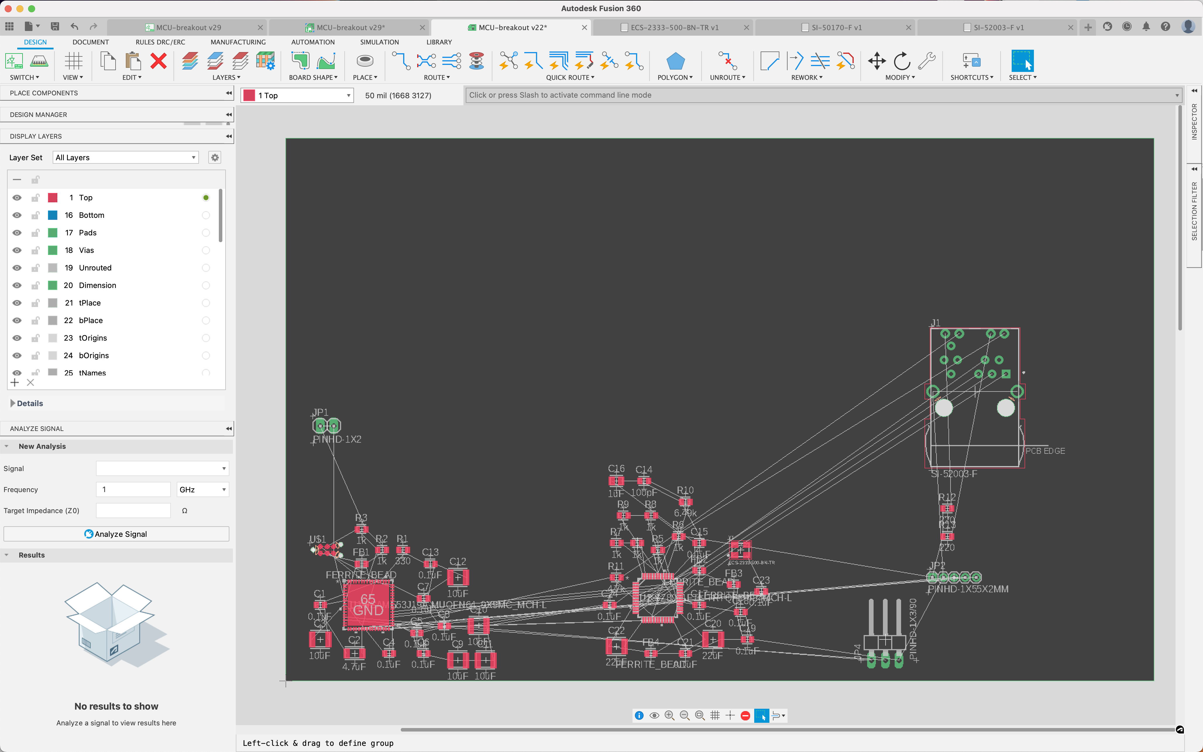
My next step here would be to pretty tightly compress all of the components physically as much as I can - this doesn’t make assembly really any harder, and since this will be a 4-layer board, at $10 per square inch, I’m aiming at saving board space (and stencil space!). I immediately notice I’ve laid down a duplicate 1k pull-up on the SWCLK pin, so took that out. After that - it’s just moving things part-by-part close in to the pins of the MCU. A couple things don’t have to be - like the SWCLK pull-up which I just moved to near the programming header. I’m sure the giant 10uF capacitors are blocking tons of signals that we’ll need later, but they’ll be OK to move back when the time comes - we’ll just send those signals to the back of the PCB close to the MCU (maybe not for the high-speed RMII signals and clocks though - it’s best to avoid vias for things like that). I also noticed that most of the I2S and RMII signals are on the bottom side of the MCU - so I just grab the whole shebang and rotate it 90o so that it faces the PHY.
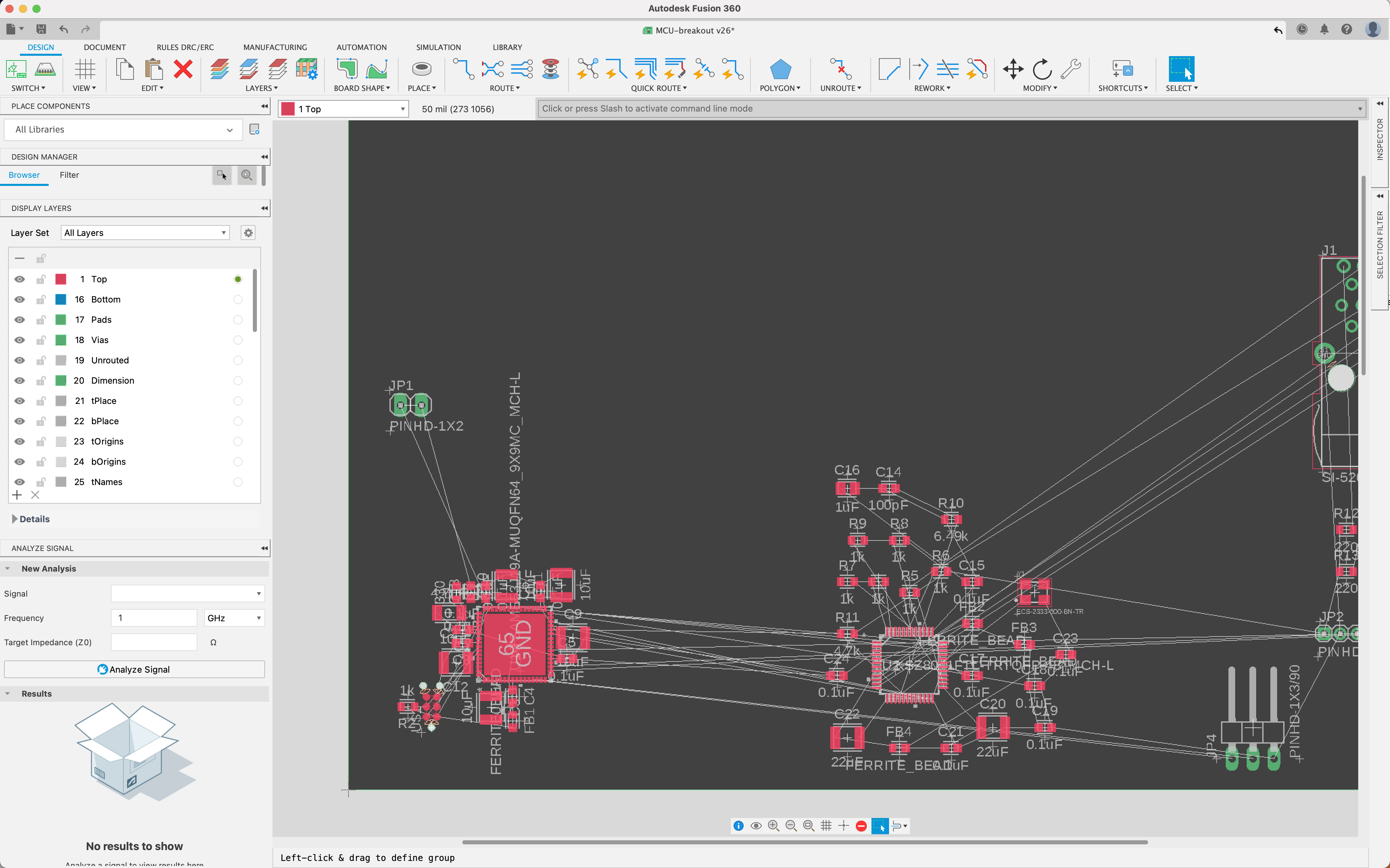
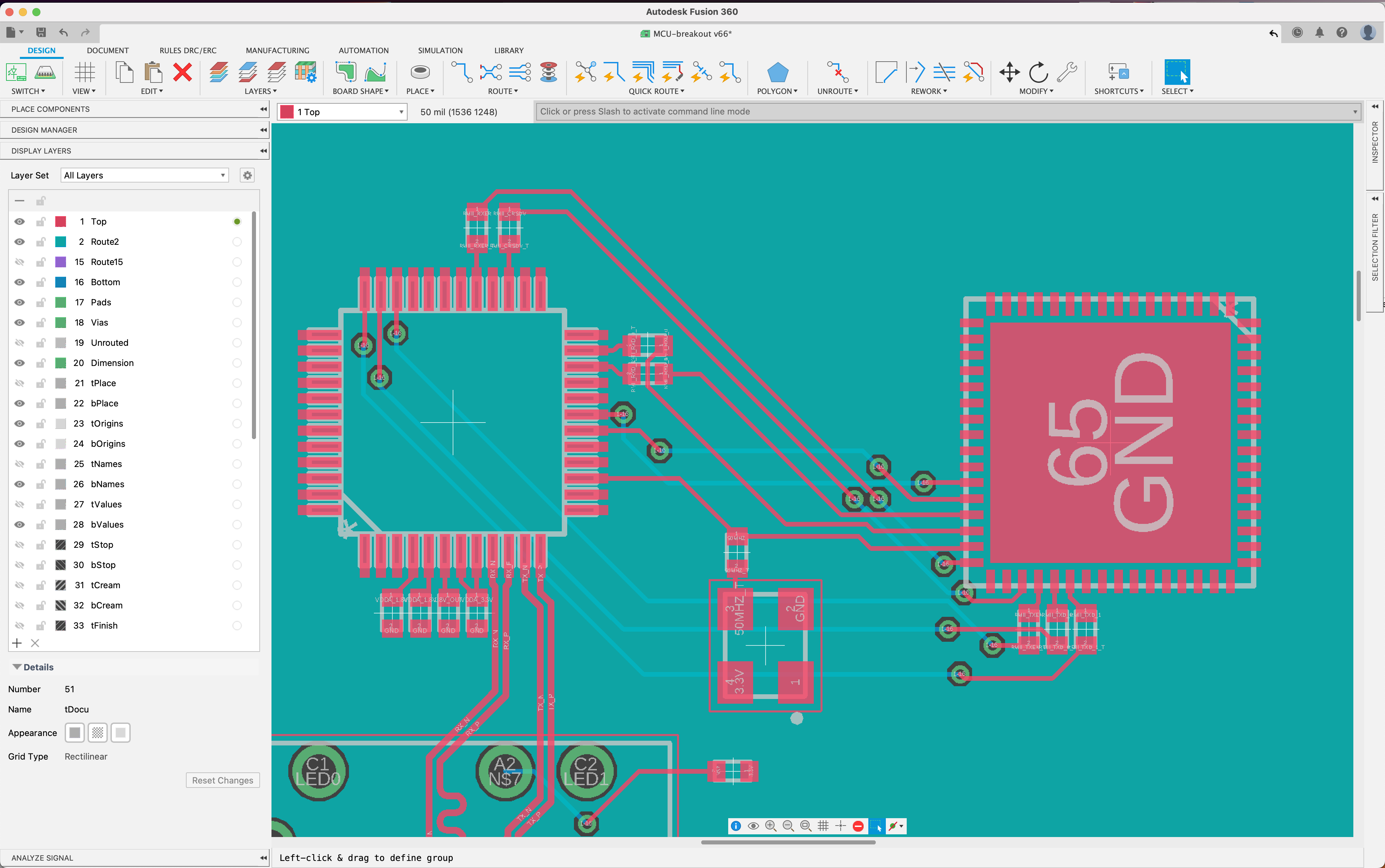
Now for the PHY. First thing I’ll do is make sure the RMII signals face the MCU before I lay out anything else.
….and, some pain here. The signals are in the wrong places:
The problem here is that I really wanted to escape all 3 groups of high-speed signals - the MAC<->PHY RX lines, MAC<->PHY TX lines, and the actual analog signals from the PHY to the RJ45 jack - on the top layer, without vias. But the way they are oriented here, there’d be no way to do this (The TX lines are the ones going to the top left corner of the PHY, the RX lines to the top right, and the lines to the jack are on the bottom right). This led me to some googling about the tolerance of RMII signals to things like vias - high-speed signals aren’t really my forte, neither are analog signals, and this challenge has both.
What I found was something that I should have looked for from the beginning - a specific hardware design checklist for the KSZ8041TL! This has all of those things I need - and it’s a new thing to walk through to make sure my schematic is complete (hint: it definitely is not).
Schematic Updates
As a result of going through this I learn the following:
- It suggests all GNDs go to the same GND plane. I had been thinking I might need a separate analog GND, but now I won’t.
- It gives recommendations for the characteristics of the ferrite beads and bulk capacitors that I should double-check against.
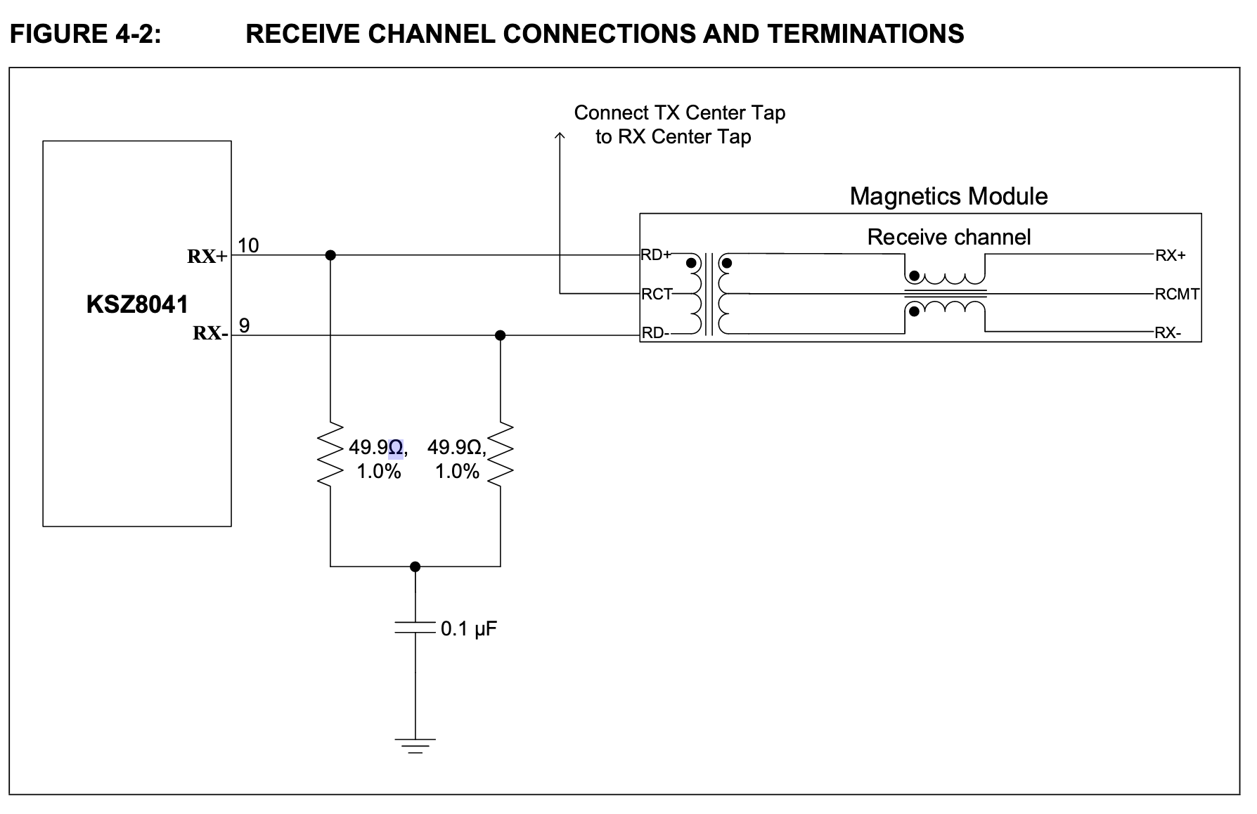
- For the PHY interface, it notes that the TX and RX center taps on the PHY side should be connected - according to the MagJack datasheet, they are internally, but I should connect them to 3.3V with an additional 10uF capacitor to ground. Added!
- It also wants 49.9Ω resistors to a 0.1uF capacitor to ground on each TX+/- and RX+/- line:
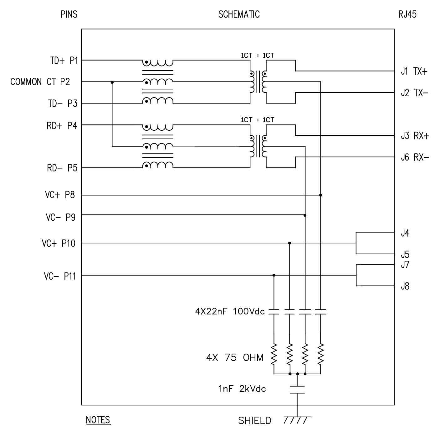
- It calls for 75Ω resistors and 1nF capacitors to GND on each of the port-facing center taps - luckily that’s handled internally to the MagJack:
- It makes clear that the 50MHz oscillator is also meant to provide a reference clock back to the MAC (in the MCU). I had an RMII_REFCLK net on the MCU that it doesn’t look like I hooked into anything; so I’ll just rename that to the 50MHz net that’s coming from the oscillator.
- It suggets 33Ω series resistors on … sigh … every RMII line, and it gives placement hints for each - some close to the clock, some close to the MAC, and some close to the PHY. So that’s 8 33Ω resistors.
- It lets you know what to do with unused input pins TXD3 and TXD4 - they should be tied to GND.
As part of laying out the series resistors - I found I’d only attached a pullup to the RMII CRSDV pin on the PHY, for configuration, instead of actually also connecting it to the CRSDV pin on the MCU. Whoops! The beauty of checking your work again and again.
Back to Layout
We’ve made a big mess now with those new series resistors. What I think I’m going to do is bite the bullet and assume that we’re going to route one RMII lane, either RX or TX, on the bottom layer. To minimize the analog crud, which I don’t understand all that well, I’m going to focus on keeping the analog traces short from the PHY to the jack, and build everything else around that.
Judging from an app note I found on Microchip’s site on gigabit ethernet routing - which is basically a superset of this - these should be routed as differential pairs, with 100Ω impedance, which is going to basically affect trace width. This is something we can calculate online using the specs of the stackup according to OSHPark.
I’m using a tool that was the first google hit, on everythingRF. Plugging in the trace thickness (1.7mil), the dielectric thickness (7.96mil - this is the PCB substrate between the top and second layer, which will be a uniform ground plane), the dielectric constant (3.61) and the smallest trace spacing (5mil), I find that an 8mil-wide trace gets me the differential impedance I’m looking for (well, within 1% of it).
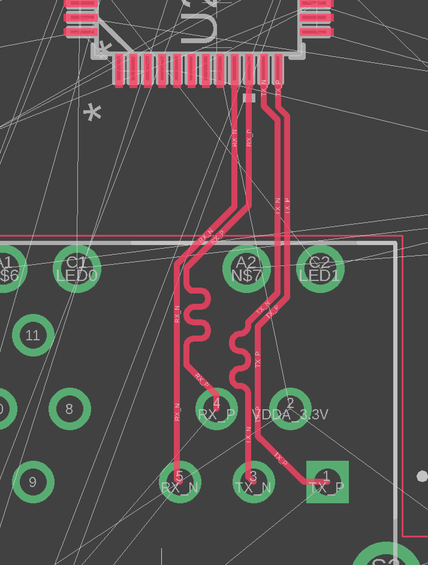
I also have to rename my signals - Fusion 360 can help with routing differential pairs, but you need to tell it that they are, by putting _N and _P as suffixes on the net names.
I’d like to length match these differential pairs - a bit overkill - this requires some use of the command line in Fusion. ‘RUN LENGTH RX_N’ and ‘RUN LENGTH RX_P’ tell me that RX_N is longer, at 15.074mm. Then opening up the ‘meander’ tool, clicking on the top of the section of RX_P that’s going to have the meander (according to another app note I read, length-matching meanders should be near the un-matched side, not the matched side, which is the pins at the PHY), right-clicking to switch to an asymmetrical meander (only one wire), and then frantically and randomly waving the mouse around, I end up here:
I swear - by all accounts, the KiCAD interface for differential pairs and meanders is way better. How could it not be? I think I really ought to consider trying KiCAD again.
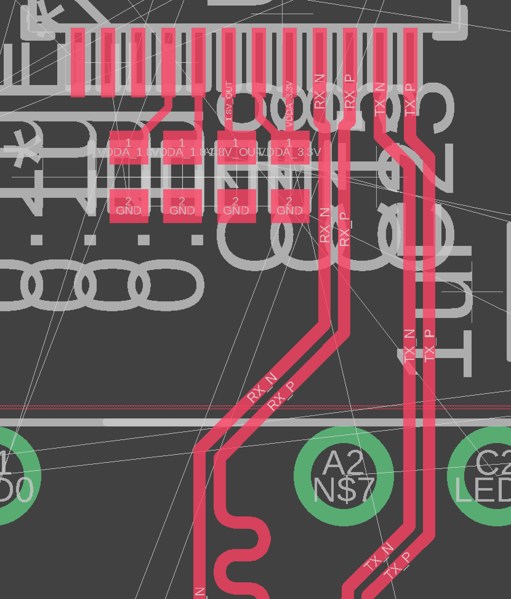
So many power pins on the bottom side of this IC though. Pins 4, 5, 6, 7, and 8 all need decoupling caps on them. With such a tiny pin pitch, this feels too crowded - the one farthest to the left is too far from the input pin that it’s supposed to support. Swapped out for 0402s, inestead of 0603s, looks a little better (the app note PDF indicates 0603 or smaller):
Honestly, as I look at this further, I’m going to bite the bullet and do a PCB-wide passive component size-shrinking pass. Resistors should be fine to move to 0402 across the board - I’ll have to buy them, but generally for resistors the formula is relatively simple: smallest possible size that can sink as much wattage as you need (and these are all extremely low power), and that isn’t so small for your tools (pick-and-place machine, or quivery hands with tweezers). I have relatively quivery tweezer hands, but 0402 is something I’ve done before, only at 0201 did I find myself way too unreliable.
Capacitor Shopping
For capacitors it’s a different story, because their effective capacitance lowers at higher voltages. This is migitated significantly by larger packages. So - what I go for is “smallest size that has close-enough to its rated capacitance at the voltage that it’ll be handling” (3.3v and 1.8v for all of these). Most of my capacitors that I have on hand date from when I did more 5v projects (which old-school Arduino runs on). So - particularly for my bigger 10uF and 22uF ones, I wonder if I can go down from the mega-huge 1210 size? Same goes for my 0805 1uF and my 0603 0.1uF.
This isn’t something that you can exactly search for on Digikey, but I’ve found that Samsung has excellent datasheets for its capacitors. I’m going to find some new SKUs for 0.1, 1.0, 10, and 22uF. Well - I already have a ton of 0402 0.1uFs, so not those. Starting from Samsung’s basic MLCC search and selecting X7R (recommended in most datasheets), 1.0uF, and ‘in production’, I get 2 hits at 0402:
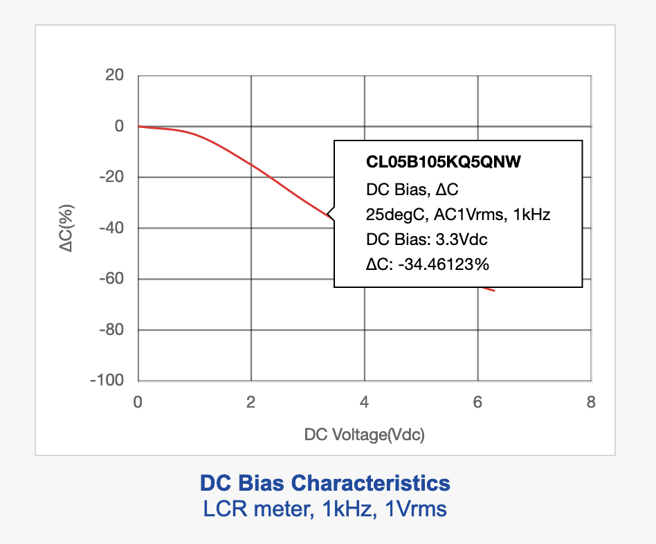
But these two each have about a ~35% derating from 1.0uF at 3.3V:
There are 30 options at 0603 though - I’m hoping that’s where I can end up. I’ll actually start by going back to Digikey and seeing what’s in stock at this size and capacitance from Samsung, that’ll help narrow it down.
Digikey has just 11 in stock, +-10% (rather than +-20%) tolerance, 1uF, Samsung, 0603 capacitors:
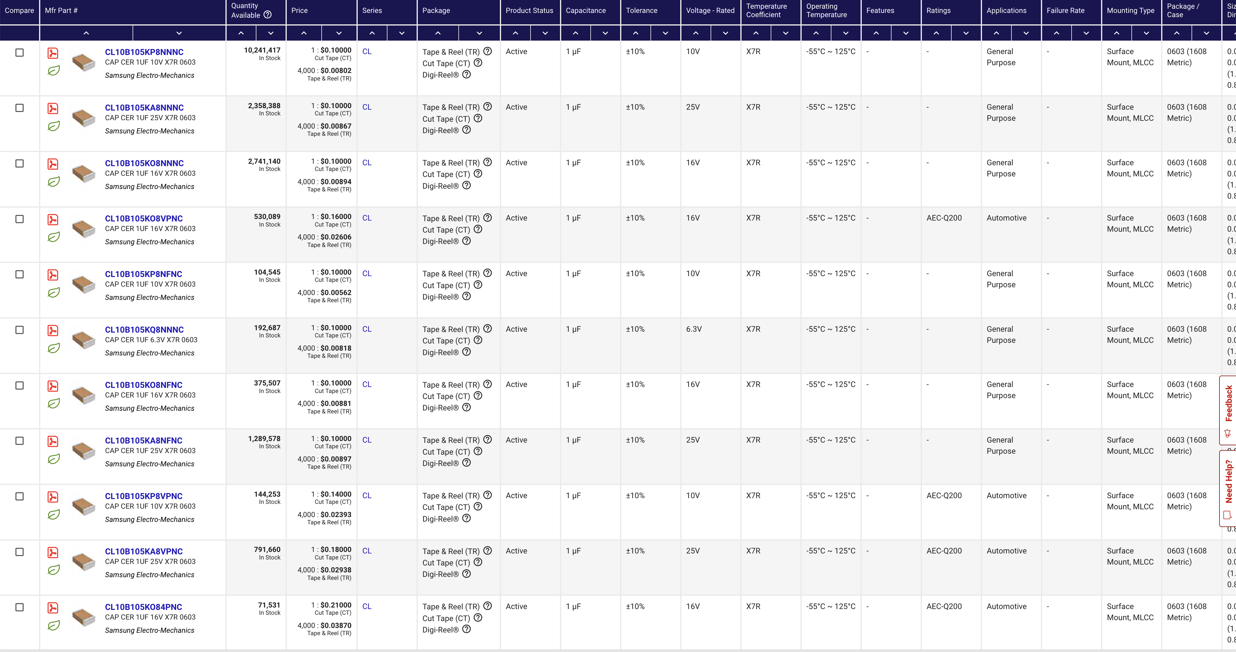
Walking down the list and checking DC bias at 3.3v:
| CL10B105KP8NNNC | -8.06% |
| CL10B105KA8NNNC | -8.76% |
| CL10B105KO8NNNC | -8.06% |
| CL10B105KO8VPNC | -7.78% |
| CL10B105KP8NFNC | -6.49% |
| CL10B105KQ8NNNC | -6.49% |
| CL10B105KO8NFNC | -6.49% |
| CL10B105KA8NFNC | -8.76% |
| CL10B105KP8VPNC | -2.99% |
| CL10B105KA8VPNC | -7.04% |
| CL10B105KO84PNC | No Data |
The CL10B105KP8VPNC seems like a winner - I’ll add it to my cart now, $4.84 for 100 of them will last a lifetime.
Now - for 10uF. There are just 2 0603s Samsung has in this rating, and a quick check of their datasheets tells me they are both about -32% derated at 3.3V - nah. I’m really hoping I can get in the ballpark at 0805. Digikey has 8 in stock - so to walk down that list here:
| CL21B106KPQNNNE | -32.50% |
| CL21B106KQQNNNE | -29.80% |
| CL21B106KOQNNNG | -29.80% |
| CL21B106KOQNNNE | -29.80% |
| CL21B106KPQNFNE | -32.50% |
| CL21B106KPQNNNG | -32.50% |
| CL21B106KQQNFNE | -29.80% |
| CL21B106KQQNNNG | -29.80% |
Well, crud. I think the secret is in the rated voltage - these are all parts rated for 10V or 6.3V, but on the Samsung site, there are ones rated for 25V, but re-checking, none are in stock at Digikey. Up to 1206 - I do find this one which is only -4.19% derated at 3.3V. That’s still a win coming down from 1210, so I’ll grab those too - $8.55 for 50 of them.
I’m discouraged that I’ll find anything smaller than 1210 at 22uF, so I won’t check. With the smaller resistors, single smaller 1uF, and several slightly-smaller 10uFs, that’ll still be helpful.
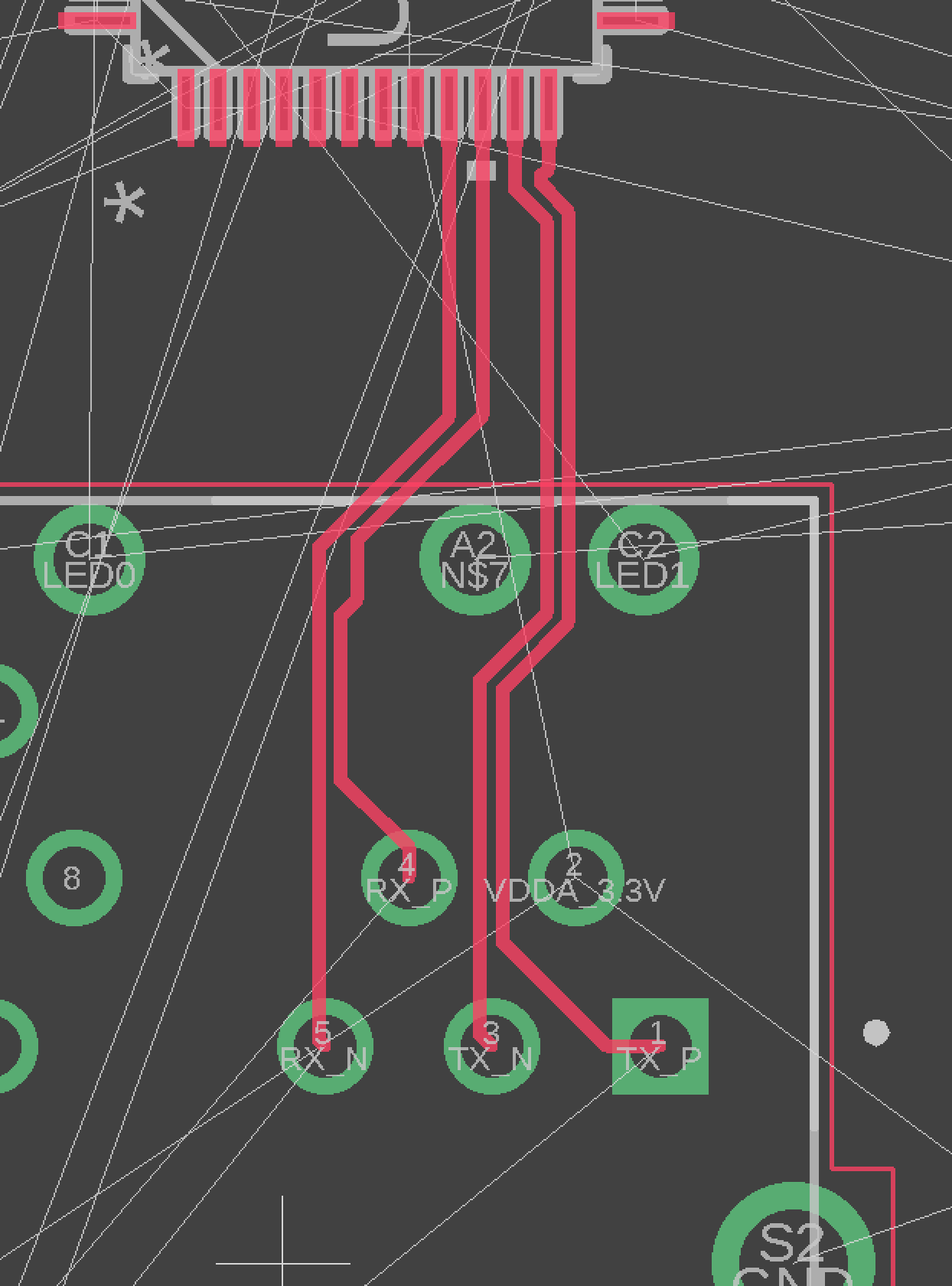
RMII trace routing
After taking a deep breath and focusing only on the 33Ω terminating resistors that have to be close to the ICs, I’ve got an initial route of the 10 RMII signals, which I absolutely hate, but is probably going to be ok?
We should do some trace length matching here. Ideally things should be more or less the same length as the reference clock signal, since they all move at its pace. I’m actually going to move the oscillator a little farther back to make that easier - it’s so close right now that there’s no room to add meanders to it.
The longest RMII trace is TXD[1], which is 30.017mm long. I’m getting a little more practiced with the meander tool now - it was relatively quick work to make everything exactly that long, including the signal from the oscillator to each IC:
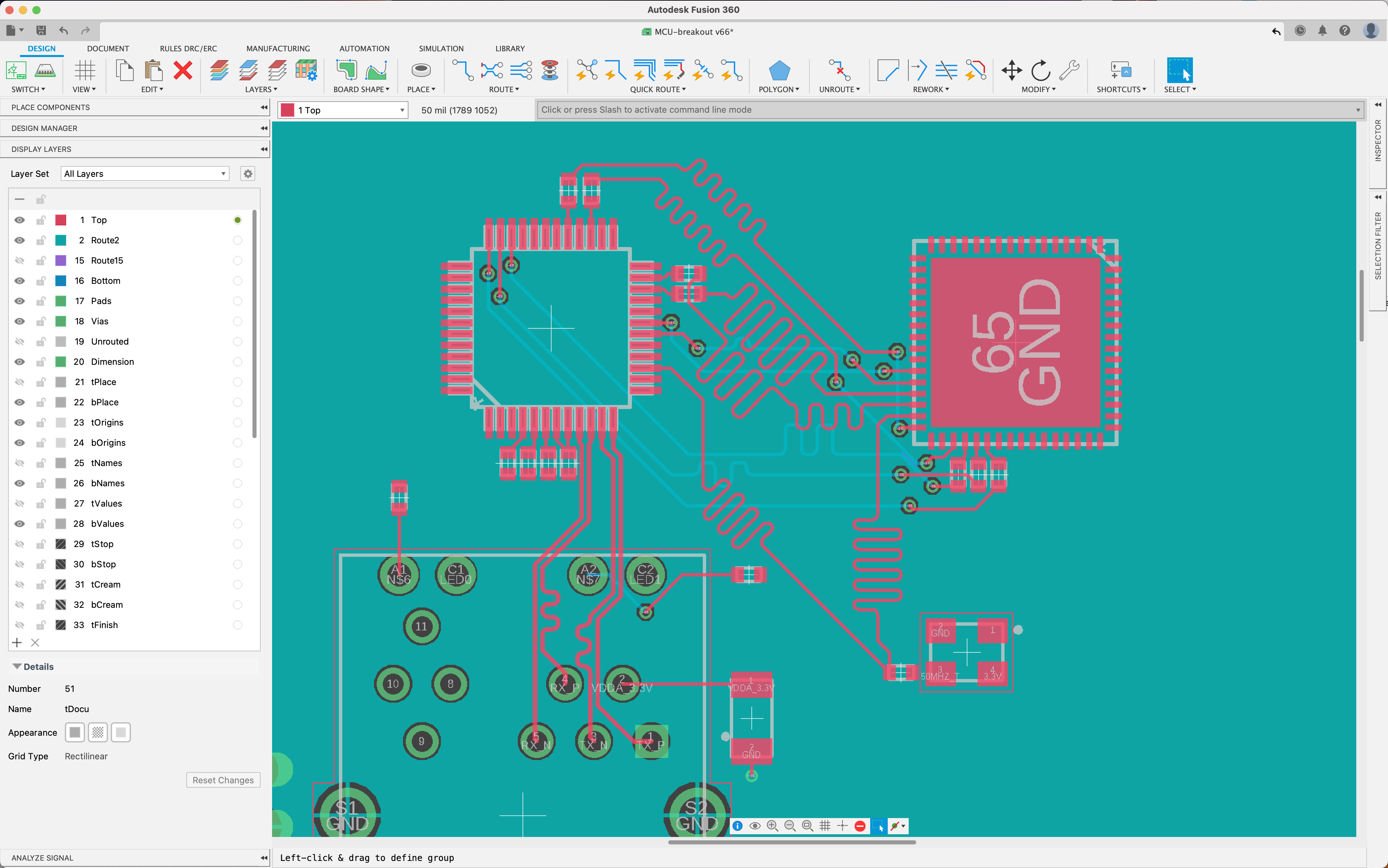
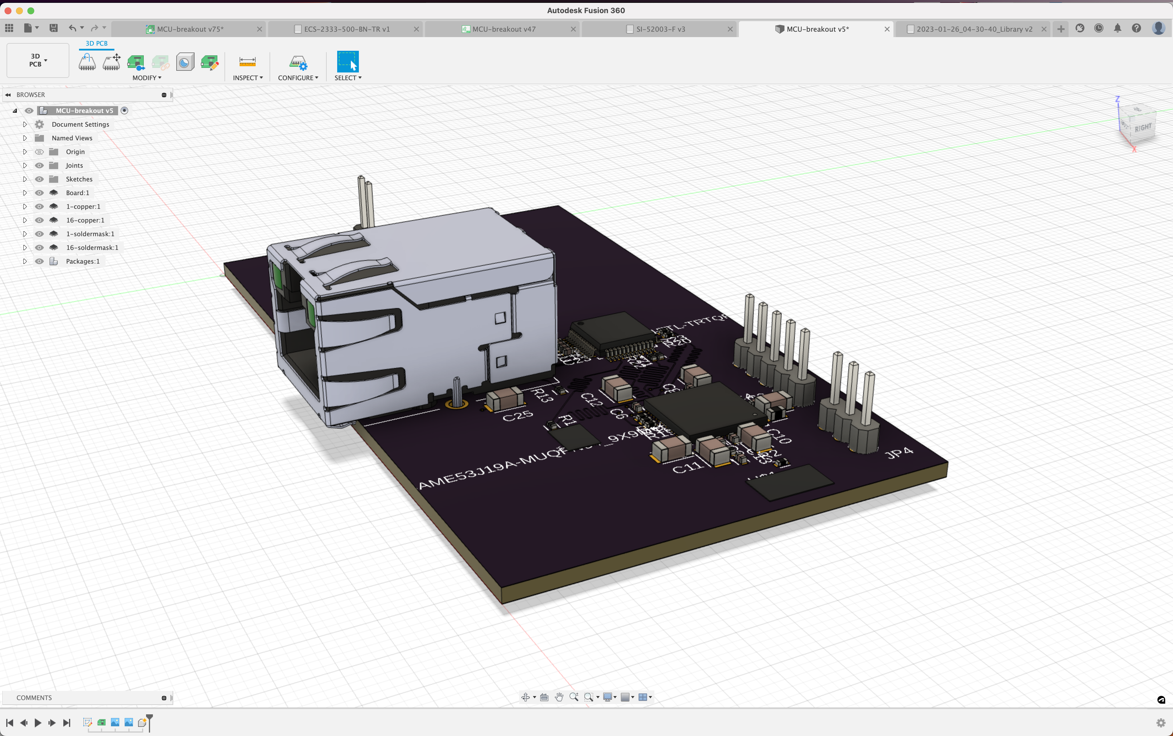
I also length-matched the MDC and MDIO on their own - that’s an independently clocked interface (MDC being the clock). After a round of bringing all the bypass and decoupling capacitors back in close to their relevant pins on the MCU, I think I’m going to call it a day - there are going to be some challenging routing issues getting the I2S signals out. The 3D view of this stopping point reminds me just how small these components are though: